Basic Definitions And References
Analog VS Digital
Electronic circuits are primarily divided into two types based on the nature of signals they process: analog and digital.
Analog circuits handle continuous signals with signals that can theoretically have an infinite number of points. However, analog signals are inherently prone to noise: disturbance caused by various factors like temperature and charge carriers. This noise, once added, becomes part of the signal, leading to an inevitable deterioration of the signal-to-noise ratio (SNR) as the signal passes through various circuit components.
Digital circuits in contrast process discrete signals, typically in binary form with values limited to “0” or “1”. They possess a noise margin that tolerates some level of noise without affecting signal interpretation. Additionally, digital circuits can regenerate signals, reducing the effects of noise.
Examples of analog vs digital signals/data
In audio processing, sampling refers to the process of recording the amplitude of a sound wave at regular intervals. An analog audio recording system could be able to capture the exact sound being emitted to it at any given moment, such as lets say for instance 3.0000000172 seconds of a recording; whereas a digital recording would sample the sound at predefined intervals. As a result, while the digital recording is still clear and recognizable to the human ear, it may not include every minute-detail of the original audio signal due to the limitations of the sampling rate. This means that the recorded sound is perceptually complete but not as “full” in reality as its analog counterpart.
Similarly, in digital photography, a camera captures a scene/video by taking a series of frames at a certain rate. Each frame is a digital snapshot of the moment, much like audio samples in digital recording. Just as a higher audio sample rate can capture more detail in sound, a higher frame rate in video can capture more detail/images and smoother motion. However, just like in audio, this doesn’t mean that every single detail present in the continuous, real-world scene is captured. The limitations of the sampling rate and resolution mean that the minute-details occurring between the frames may not be recorded.
Number Systems
Number systems are frameworks for representing and manipulating numbers. Each number system is defined by its base, or radix, which indicates the number of unique digits, including zero, that the system uses to represent numbers. For example, the decimal system, which is the most familiar system for everyday arithmetic, has a base of 10, meaning it uses ten distinct digits (0 through 9). The concept of a “digit” in any number system represents the incremental values that make up numbers.
The first time I was introduced to number systems other than decimal, the concepts that gave me the intuition was the “ticking point”. When the highest digit in a system is exceeded, the system “ticks over” to the next positional value, starting again at zero. In the decimal system, this happens after 9. When you add one to 9, you “tick over” to 10, starting a new digit place. Similarly, in the hexadecimal system, which has a base of 16 and includes digits from 0 to F (where F represents 15 in decimal), the ”tick over” occurs after F, moving to 10 in hexadecimal (which is equivalent to 16 in decimal).
The Binary/Base 2 number system, and why using it?
A “bit”, short for binary digit, is the most basic(next to unary) unit of data in computing and digital communications. It can hold one of two values, typically represented as 0 or 1, mirroring the binary system’s base of 2.
The binary system, which is the “language” of most computers, is used, not necessarily for being the superior numerical system but because it aligns with the ON/OFF nature of transistors. In layman’s terms, transistors in digital circuits(different story in analogue circuits) typically operate in a binary manner, being either in an ON state or an OFF state. Thus, binary is naturally fit to be the language of computers, as it directly corresponds to the physical state of their basic hardware components.
Below is the conversion table for numbers from 0 to 32 in decimal, binary, hexadecimal, and octal formats:
| Decimal | Binary | Hexadecimal | Octal |
|---|---|---|---|
| 0 | 0 | 0 | 0 |
| 1 | 1 | 1 | 1 |
| 2 | 10 | 2 | 2 |
| 3 | 11 | 3 | 3 |
| 4 | 100 | 4 | 4 |
| 5 | 101 | 5 | 5 |
| 6 | 110 | 6 | 6 |
| 7 | 111 | 7 | 7 |
| 8 | 1000 | 8 | 10 |
| 9 | 1001 | 9 | 11 |
| 10 | 1010 | a | 12 |
| 11 | 1011 | b | 13 |
| 12 | 1100 | c | 14 |
| 13 | 1101 | d | 15 |
| 14 | 1110 | e | 16 |
| 15 | 1111 | f | 17 |
| 16 | 10000 | 10 | 20 |
| 17 | 10001 | 11 | 21 |
| 18 | 10010 | 12 | 22 |
| 19 | 10011 | 13 | 23 |
| 20 | 10100 | 14 | 24 |
| 21 | 10101 | 15 | 25 |
| 22 | 10110 | 16 | 26 |
| 23 | 10111 | 17 | 27 |
| 24 | 11000 | 18 | 30 |
| 25 | 11001 | 19 | 31 |
| 26 | 11010 | 1a | 32 |
| 27 | 11011 | 1b | 33 |
| 28 | 11100 | 1c | 34 |
| 29 | 11101 | 1d | 35 |
| 30 | 11110 | 1e | 36 |
| 31 | 11111 | 1f | 37 |
| 32 | 100000 | 20 | 40 |
Nibble, Bytes, Words Notations and Conversions
1 nibble = 4 bits = $2^4$ = 16 different numbers (0 to 15)
1 byte = 8 bits = $2^8$ = 256 different numbers (0 to 255)
Nibbles are rarely utilized in engineering. Whether in software development, technical documentation, or everyday communication among engineers, the byte is the more commonly referenced unit.
Processors operate on data units known as words. The size of a word varies depending on the microprocessor’s architecture. Most computers nowadays use 64-bit processors, meaning their word size is 64 bits. In contrast, microcontrollers like Arduino and STM boards typically use 32-bit processors, suitable for their less demanding processing tasks.
In programming languages, non-decimal numbers are typically written with specific prefixes to indicate their base:
Binary numbers use the prefix 0b. Ex: 0b1010 for the binary representation of 10.
Hexadecimal numbers use 0x. Ex: 0x1A for the hexadecimal representation of 26.
Octal numbers use 0. Ex: 034 for the octal representation of 28.
Binary to Decimal to Binary
To convert a decimal number to binary, divide it by 2 until you get to 1. If you have an odd number, take the next number below it and divide it by 2. For every odd number obtained in the division, write 1, and 0 for every even number, from left to right.
Converting Decimal to Binary:

Example: Convert 13 to binary.

1. 13 / 2 = 6, remainder 1 (write down 1)
2.  6 / 2 = 3, remainder 0 (write down 0)
3.  3 / 2 = 1, remainder 1 (write down 1)
4.  1 / 2 = 0, remainder 1 (write down 1)

Binary representation: 1101
To convert back to decimal, raise 2 to the power of every 1s position in the binary number, again, counting from left to right.
Converting Binary to Decimal:

Example: Convert 1101 (binary) to decimal.

1. Rightmost digit ($2^0$ position): 1 * 2^0 = 1
2. Next digit (2^1 position): 0 * 2^1 = 0
3. Next digit (2^2 position): 1 * 2^2 = 4
4. Leftmost digit (2^3 position): 1 * 2^3 = 8

Decimal sum: 1 + 0 + 4 + 8 = 13
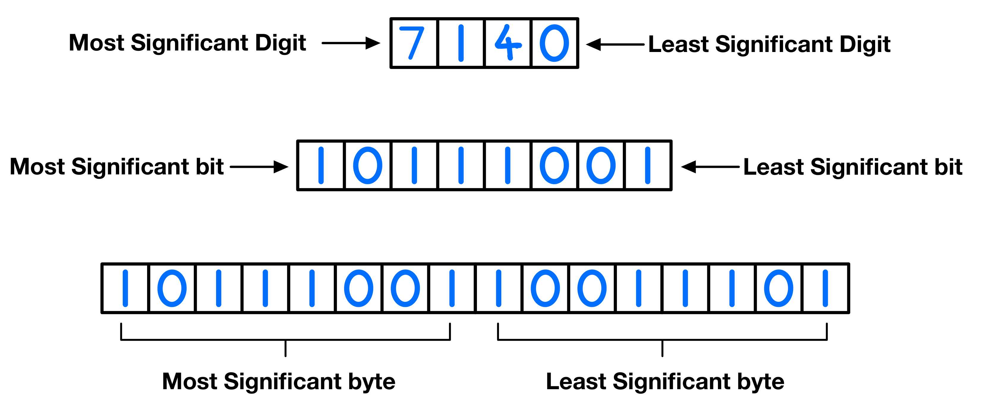
Least/Most Significant Value
Least Significant Bit/Byte (LSB):
Position: Rightmost bit/byte in a binary number.
Most Significant Bit/Byte (MSB):
Position: Leftmost bit/byte in a binary number.
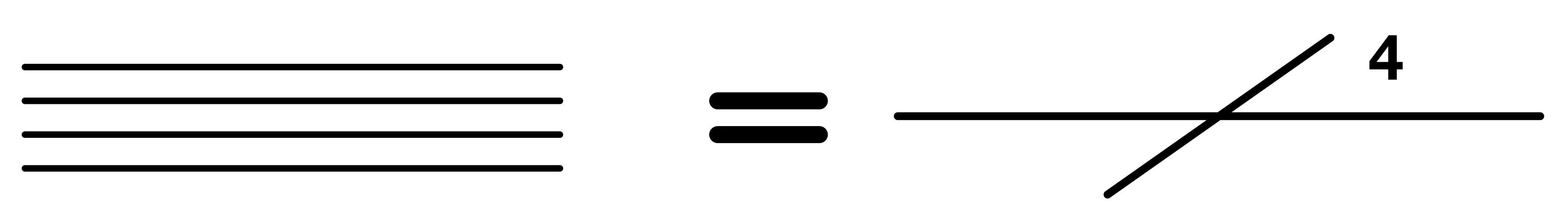
Bus
A bus is a shared data pathway that various components of a processor use to communicate with each other. It is typically represented by a slanted line (like a forward slash), with a number above it indicating the data pathway’s width, or the number of data lines it contains. This representation condenses the depiction of multiple data wires into a single bus illustration.

The example below shows a bus with four data lines.
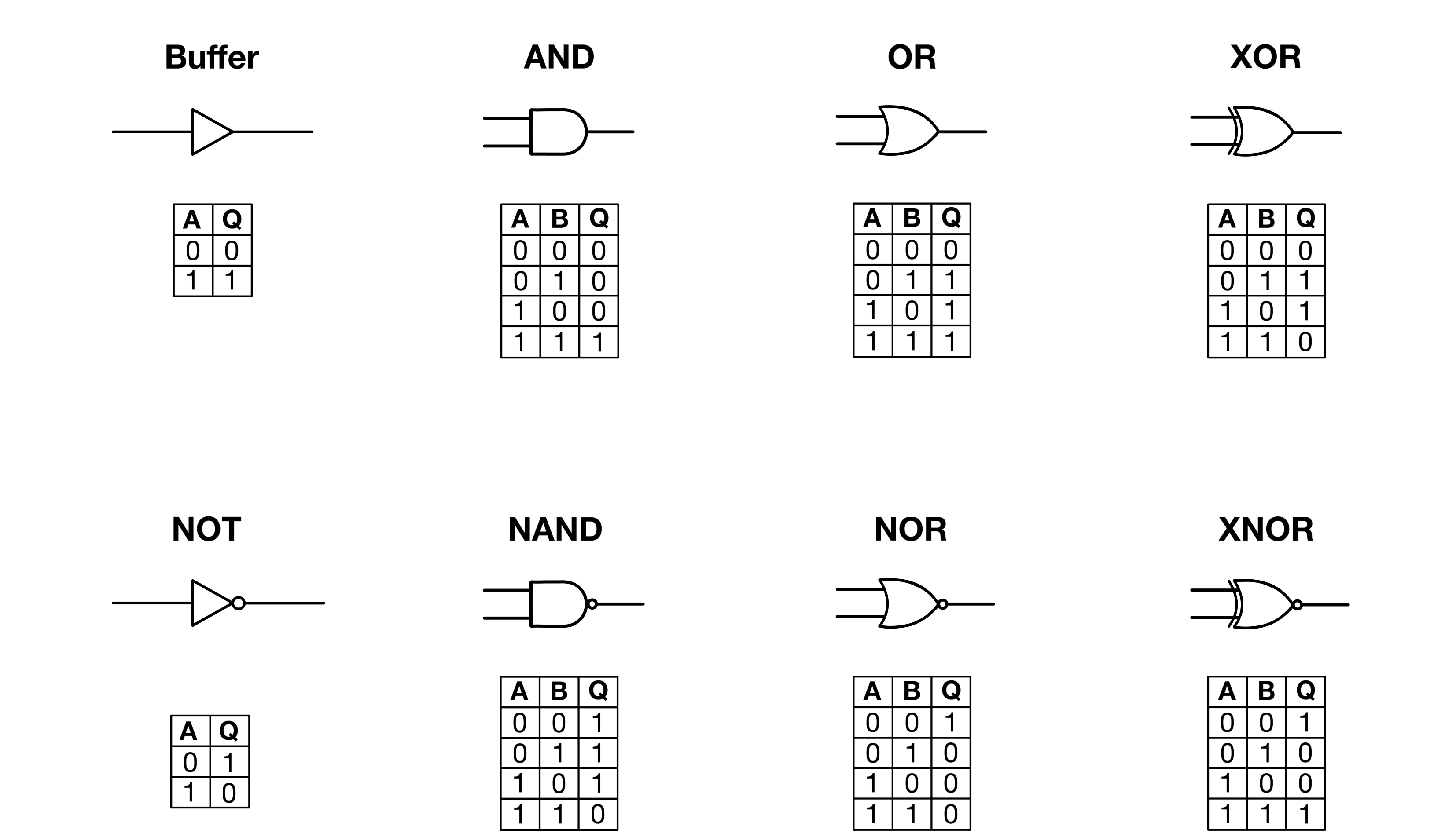
Logic Gates
Logic gates are the fundamental building blocks of digital electronics! They are devices that perform logical/Boolean operations on one or more binary inputs to produce a single binary output. These operations are basic to digital computing and are used in creating complex circuits that perform a variety of tasks.
Basic Logic Gates:
- AND Gate: Outputs a “True” (1) value only if both inputs are “True”.
- OR Gate: Outputs a “True” value if at least one input is “True”.
- NOT Gate (Inverter): Outputs the opposite of the input value.
- NAND Gate: Outputs a “False” (0) value only if both inputs are “True” (the inverse of the AND gate).
- NOR Gate: Outputs a “False” value if at least one input is “True” (the inverse of the OR gate).
- XOR Gate (Exclusive OR): Outputs a “True” value only if the inputs are different.
Each logic gate type has a corresponding truth table, which lists all possible input combinations and their respective outputs. Truth tables are essential for understanding how logic gates operate and for designing complex circuits.
Truth Tables:
A truth table is a mathematical table used in logic, specifically in connection with Boolean algebra, Boolean functions, and propositional calculus, to compute the functional values of logical expressions on each of their functional arguments. For instance, the truth table for an AND gate is:
| Input A | Input B | Output (A AND B) |
|---|---|---|
| 0 | 0 | 0 |
| 0 | 1 | 0 |
| 1 | 0 | 0 |
| 1 | 1 | 1 |
Here, “0” represents “False” and “1” represents “True”. The output column shows that the AND gate only returns “True” when both inputs are “True”.
Combinational Vs Sequential Circuits
A simple way to understand the difference between sequential and combinational circuits, at least initially, is to think of them in terms of states.
Combinational circuits, just like an $f(x) = y$ function, output values based solely on their current inputs, without memory of past states.
Sequential circuits, on the other hand, rely on both current and past inputs. In other words, the next output of a sequential circuit not only depends on the set of inputs that can generate it, but also on the state of the circuit as the input is being entered.
Another way to look at the difference between sequential and combinational circuits is: In a combinational circuit, if you were to hide the input and only look at the output; you’d be able to tell the input(Or the set of possible inputs), because it has a know corresponding output; but in a sequential circuit, an input cannot be determined simply by looking at the current output.
Pull Up & Pull Down Resistors
Pull-up and pull-down resistors are used to ensure a specific and stable logic level (HIGH or LOW) at a pin in the absence of an input signal:
Pull-up resistors connect the pin to a HIGH voltage level, serving as a logical HIGH when not actively driven.
Pull-down resistors do the opposite, connecting the pin to ground to ensure a logical LOW state.
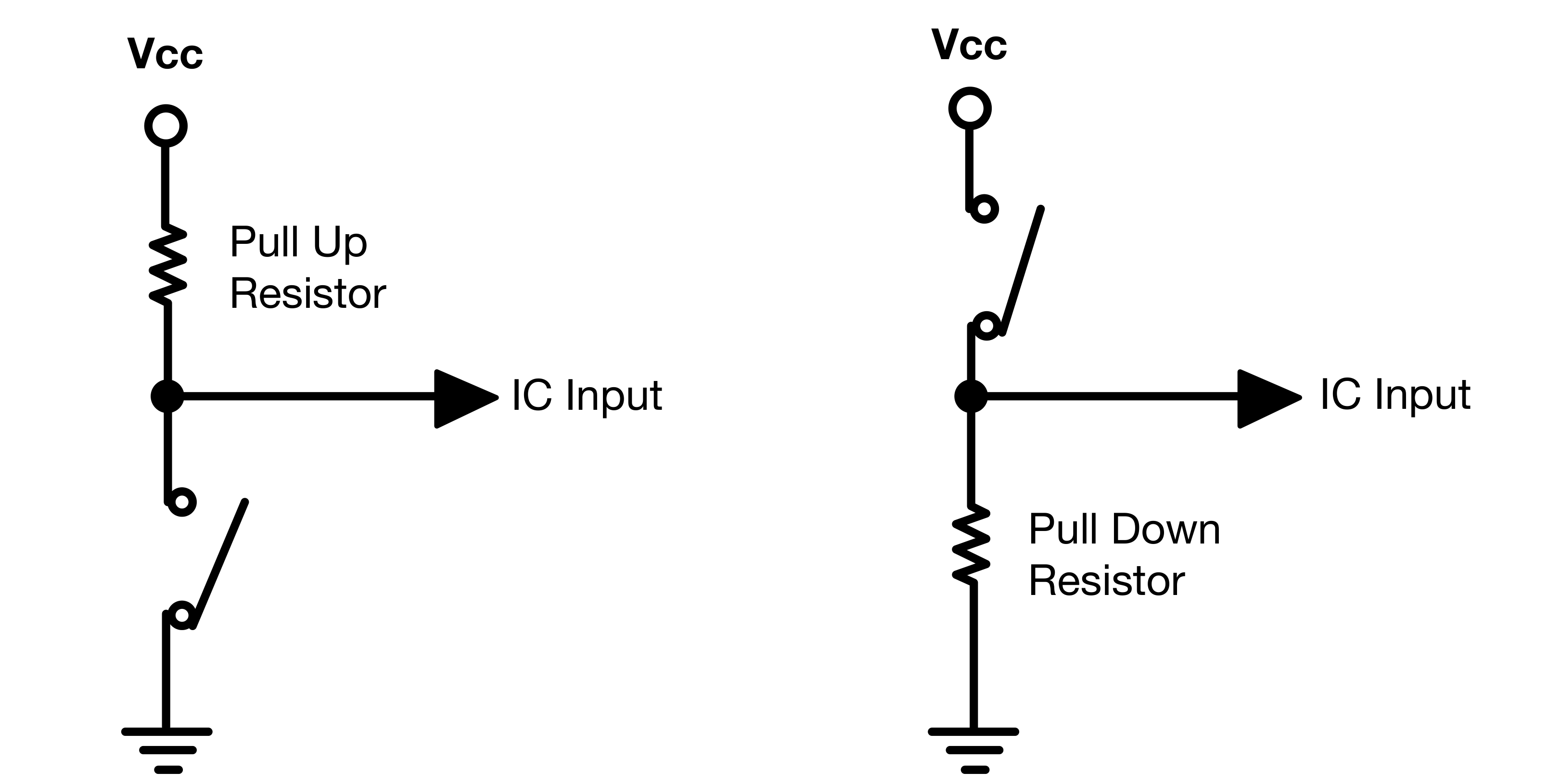
The value of the resistors should be high enough to prevent excessive power consumption and low enough to ensure a clear signal. While it is ideal to select a value based on specific application needs and the characteristics of the input pin, such as its impedance and leakage current, a general guideline for situations where detailed information is not available, is to use values between 1kΩ and 10kΩ, which are typically suitable for most microcontroller applications.
Floating State: Understanding Logic Levels
Beside the need in some cases, to purposely have a specific state at an input pin when unused, there is more importantly the issue of floating inputs in digital circuits; which occurs when a logic gate input is neither driven to a logical high nor a logical LOW, leaving it in an undefined or “floating” state. This undefined state is problematic because it makes the input susceptible to noise and stray electromagnetic fields, which can cause the input at a gate to be randomly interpreted as HIGH or LOW and in turn lead to erratic behavior.
Logic levels are the defined ranges of voltages that correspond to binary states.
VOH : Minimum output voltage level a device will provide for a HIGH signal.
VIH : Minimum input voltage level to be considered a HIGH.
VOL : Maximum output voltage level a device will provide for a LOW signal.
VIL : Maximum input voltage level to still be considered a LOW.
A driver gate outputs these levels, with a LOW (0) output ranging from 0 to VOL and a HIGH (1) output from VOH to VDD. Correspondingly, a receiver gate interprets inputs within the range of 0 to VIL as LOW and those from VIH to VDD as HIGH. However, if the input falls into the “forbidden zone” between VIL and VIH, the gate’s behavior becomes unpredictable. Therefore, to ensure reliable communication between the driver and receiver, the noise margin must be considered.
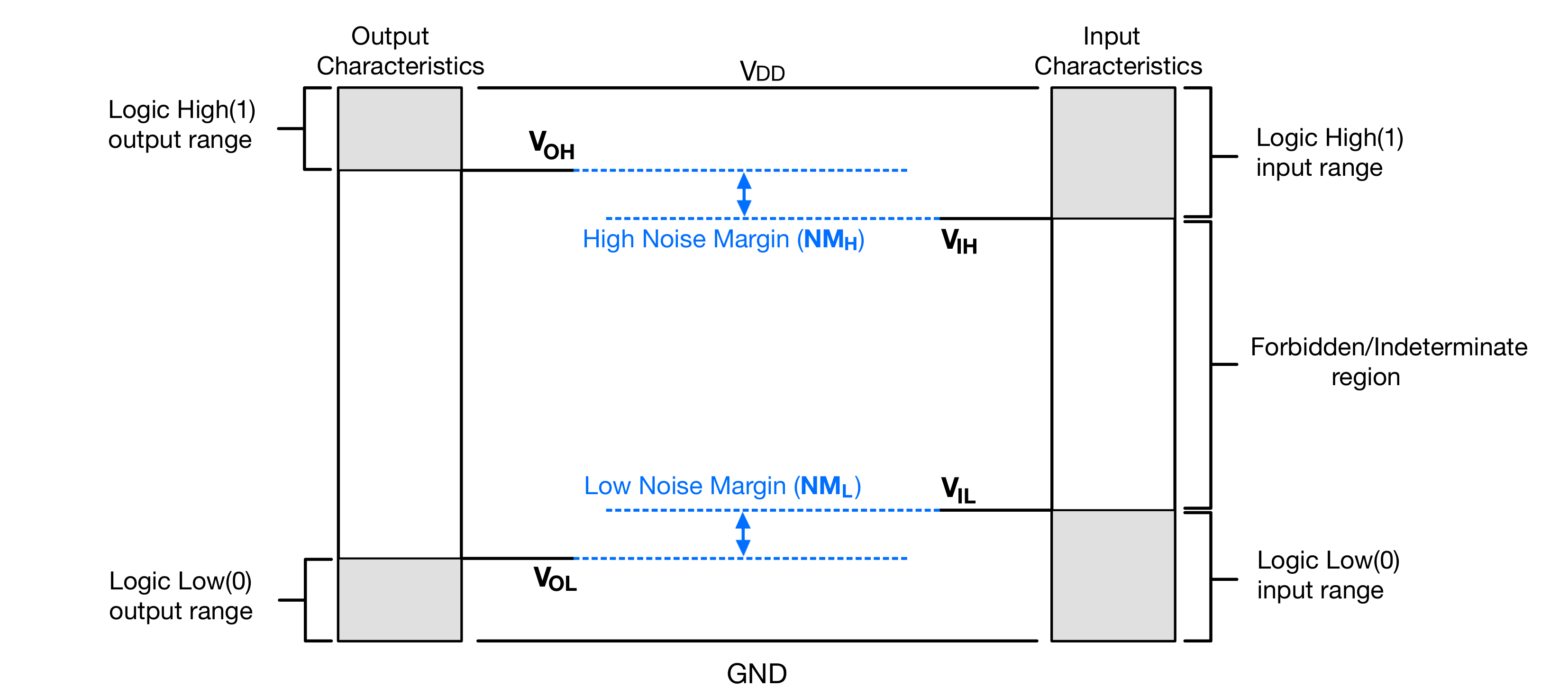
The noise margin defines the permissible range of noise that can be superimposed on a signal without affecting its interpretation. For correct logic level interpretation, it’s essential that VOL be less than VIL and VOH be greater than VIH, to provide a buffer against noise. The low and high noise margins are quantified as:
$NML = VIL - VOL$
and
$NMH = VOH - VIH$
together representing the tolerance of a system to potential signal disturbances.
Logic levels are not fixed but largely dependent on the semiconductor materials and manufacturing techniques used in creating the logic gates. This means that gates within a circuit must share compatible logic levels to function properly. Consequently, gates are organized into logic families (ex: TTL, CMOS, LVCMOS…), where each family adheres to a consistent electrical standard. When mixing gates from different families, however, there’s a significant risk of incompatibility due to the differing voltage and logic level requirements, potentially leading to malfunction or inefficiency in the circuit.
Switches: Poles and Throws
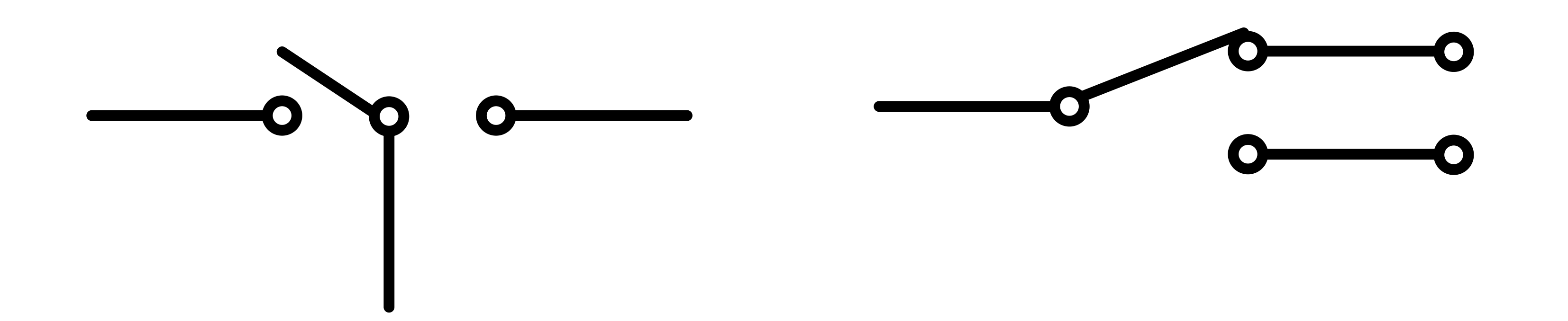
Switches are fundamental components in electronics, and are used to make or break electrical connections in a circuit. Understanding switches often involves terms like “poles” and “throws”, which describe the configuration of the switch.
Poles
A “pole” refers to the number of separate circuits that a switch can control. In other words, it’s the number of electrically separate contacts that a switch has. If a switch has one pole, it means it can control one circuit (one set of contacts). For example, a single-pole switch can make or break the connection in a single circuit.
Throws
A “throw,” on the other hand, refers to the number of positions that each pole can connect to. This determines how many states or positions the switch can adopt. For example, a single-throw switch (ST) has one position that the pole can connect to, while a double-throw switch (DT) has two possible positions.
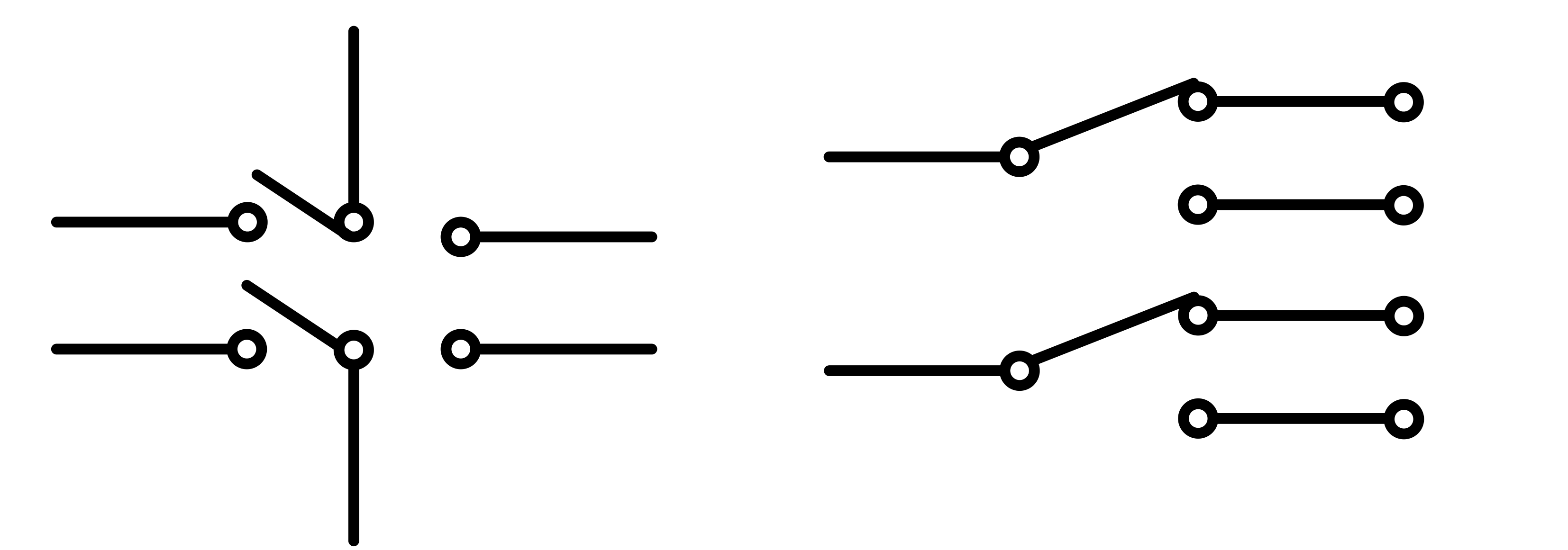
Some Types of Switches Based on Poles and Throws
1- Single Pole Single Throw (SPST): This is the simplest type of switch, with one pole and one throw. It acts as a simple ON/OFF switch that controls a single circuit. Examples include light switches and power switches on basic electronic devices.

2- Single Pole Double Throw (SPDT): This switch has one pole and two throws. It can connect a single input circuit to one of two output circuits. SPDT switches are often used in applications where switching between two circuits is necessary, like selecting between two power sources.
3- Double Pole Single Throw (DPST): A DPST switch controls two separate circuits but only has one throw. It’s like having two SPST switches operated by a single mechanism. This type of switch is used where two circuits need to be turned on or off simultaneously.

4- Double Pole Double Throw (DPDT): This has two poles, each with two throws. It’s essentially two SPDT switches operated together. DPDT switches are common in applications that require reversing the direction of motors or in complex circuitry where control of two lines is needed simultaneously.
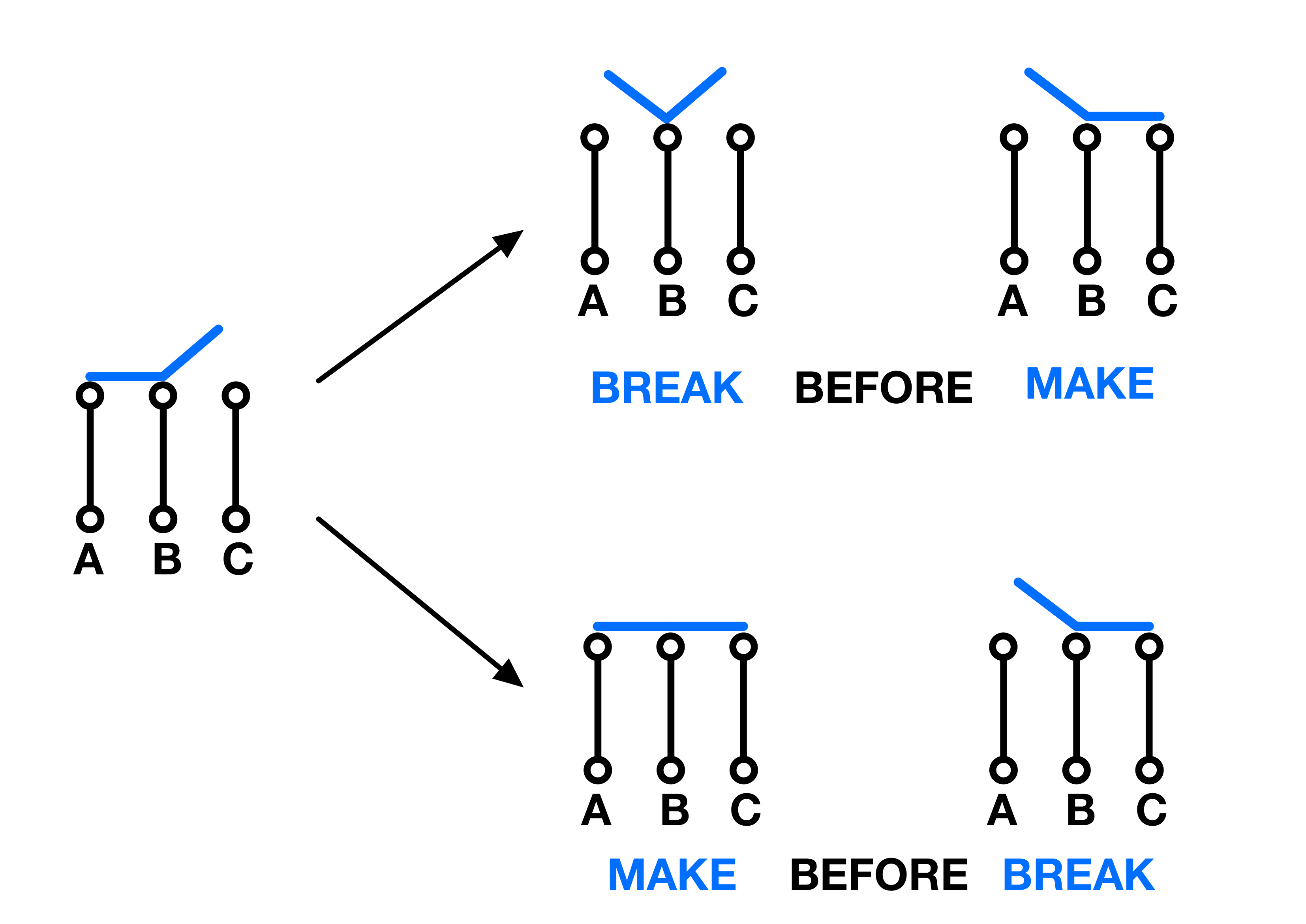
Make Before Break and Break Before Make Switches
“Make Before Break” and “Break Before Make” are terms that describe how the contacts within a switch operate during the transition from one position to another. These characteristics are particularly important in multi-position switches, such as rotary or slide switches, where the switch might move between different states or connections.
Make Before Break
A “make before break” switch is designed so that the new contact is made (connected) before the old contact is broken (disconnected). This means that, during the switching action, there is a brief moment when both the old and new contacts are simultaneously connected.
Break Before Make
A “break before make” switch, conversely, breaks contact with the current position before making contact with the new position. There is a brief moment during the switch action when neither contact is connected.
Consider Nodes A, B, and C in the image below. The steps on the right show the intermediary step of a BBM and MBB when connecting B to C.
Multiplexers
A multiplexer(mux), or data selector is a combinational circuit which can route one of several input signals to a single output using “select” signals to pick the corresponding input.
Number of inputs = $2^n$ → $n$ being the number of selects.
Number of selects = $log_2M$ → $M$ being the number of inputs.
A mux always has one output. It can be thought of as a multi-signal switch.
On the left of the image below is the symbol of an 8-to-1 multiplexer and on the right is an oversimplified representation of what is going on within the mux.
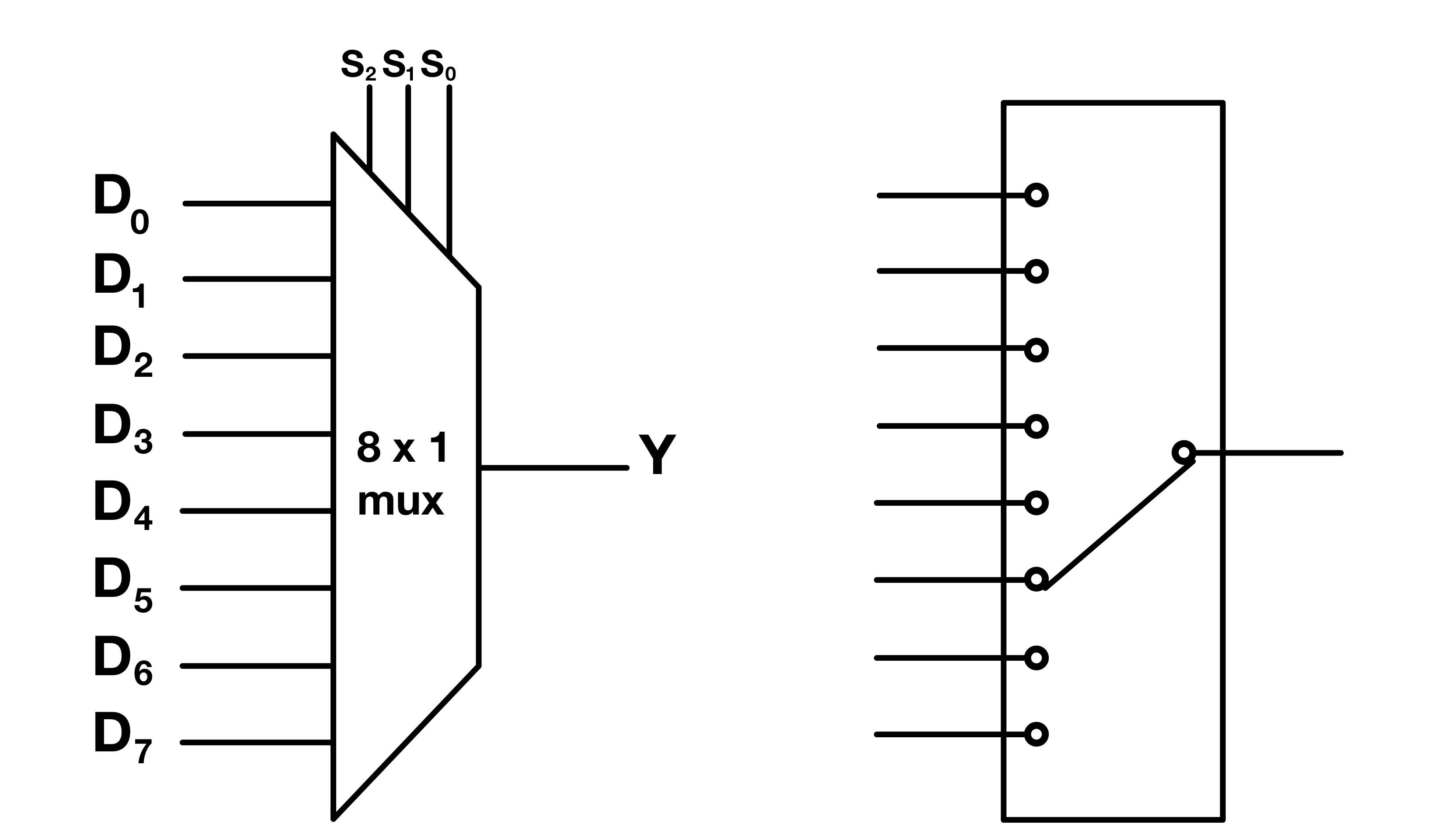
The three select lines (S0, S1, S2) determine which one of the 8 data inputs (D0 to D7) is connected to the output. There are $(2^3 = 8)$ possible combinations of select lines, corresponding to each of the 8 data inputs.
Here’s the truth table:
| S2 | S1 | S0 | Y |
|---|---|---|---|
| 0 | 0 | 0 | D0 |
| 0 | 0 | 1 | D1 |
| 0 | 1 | 0 | D2 |
| 0 | 1 | 1 | D3 |
| 1 | 0 | 0 | D4 |
| 1 | 0 | 1 | D5 |
| 1 | 1 | 0 | D6 |
| 1 | 1 | 1 | D7 |
Decoders/Demultiplexers
A decoder/demultiplexer(demux), is a combinational circuit that performs the opposite function of a multiplexer. While a multiplexer takes multiple input signals and routes them into a single output line, a demultiplexer does the reverse: It takes a single input signal and distributes it to one of several output lines. The specific output line to which the input signal is sent is determined by a set of select lines.
Number of outputs = $2^n$ → $n$ being the number of selects.
A demux always has one input.
On the left of the image below is the symbol of an 1-to-8 demultiplexer and on the right is an oversimplified representation of what is going on within it.
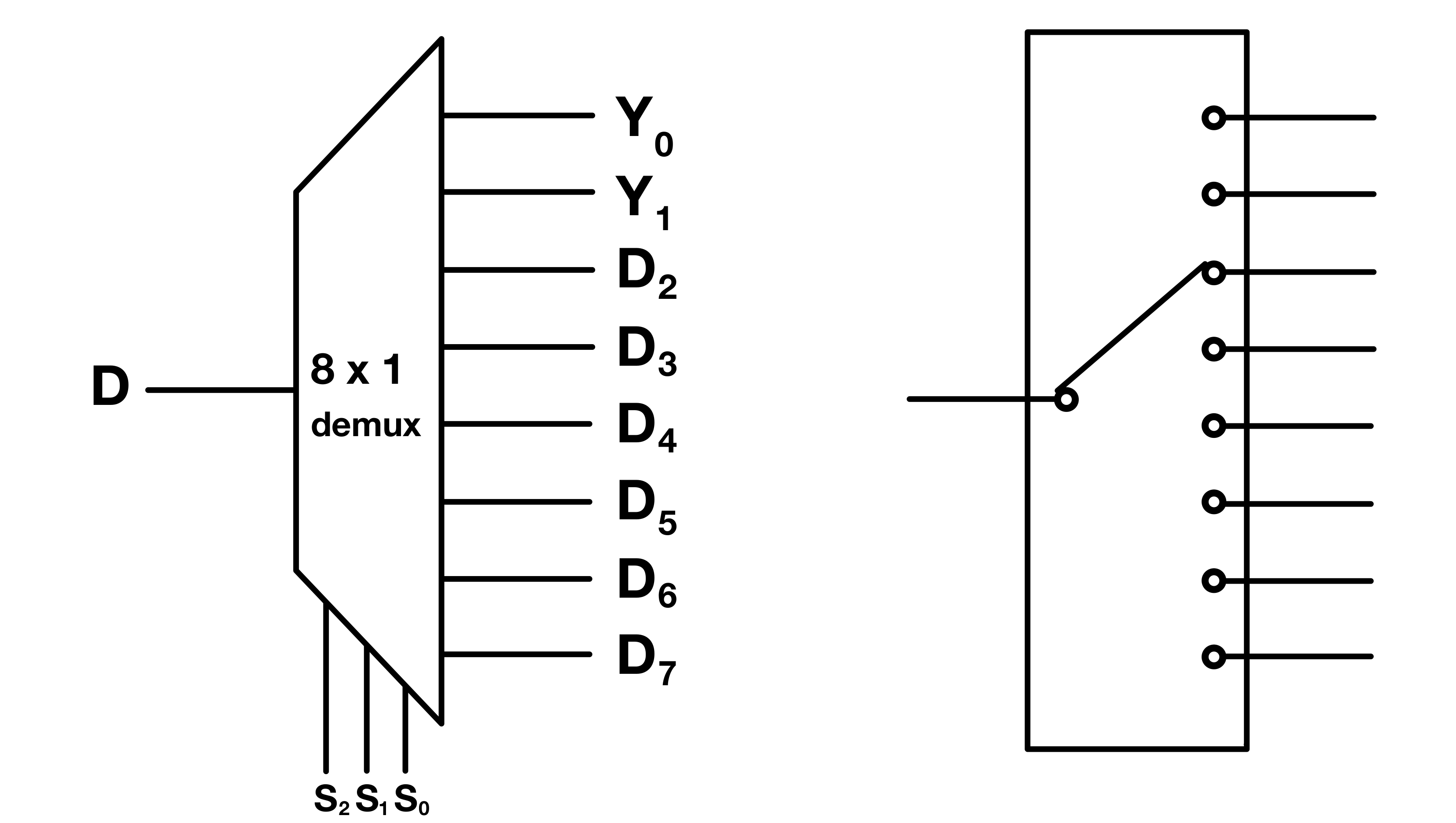
Here’s the truth table:
| S2 | S1 | S0 | Y0 | Y1 | Y2 | Y3 | Y4 | Y5 | Y6 | Y7 |
|---|---|---|---|---|---|---|---|---|---|---|
| 0 | 0 | 0 | D | 0 | 0 | 0 | 0 | 0 | 0 | 0 |
| 0 | 0 | 1 | 0 | D | 0 | 0 | 0 | 0 | 0 | 0 |
| 0 | 1 | 0 | 0 | 0 | D | 0 | 0 | 0 | 0 | 0 |
| 0 | 1 | 1 | 0 | 0 | 0 | D | 0 | 0 | 0 | 0 |
| 1 | 0 | 0 | 0 | 0 | 0 | 0 | D | 0 | 0 | 0 |
| 1 | 0 | 1 | 0 | 0 | 0 | 0 | 0 | D | 0 | 0 |
| 1 | 1 | 0 | 0 | 0 | 0 | 0 | 0 | 0 | D | 0 |
| 1 | 1 | 1 | 0 | 0 | 0 | 0 | 0 | 0 | 0 | D |
Latches
Latches are basic sequential circuits and memory elements used in digital electronics to store binary information. They can maintain their state (storing a bit) as long as power is supplied to the circuit. Latches are built using logic gates and are key components in digital systems for temporary data storage.
SR Latch
The SR (Set-Reset) Latch is one of the simplest types of latches. It is made using two cross-coupled NOR or NAND gates. The latch has two inputs, typically labeled S (Set) and R (Reset), and two outputs Q and Q’ (Q-bar, the inverse of Q).
- Set Operation: When the S input is activated (logic 1 for NOR, logic 0 for NAND), the latch sets, and the Q output becomes 1, while Q’ becomes 0.
- Reset Operation: When the R input is activated, the latch resets, making Q output 0 and Q’ output 1.
- Hold State: When both inputs are deactivated (logic 0 for NOR, logic 1 for NAND), the latch maintains its current state.
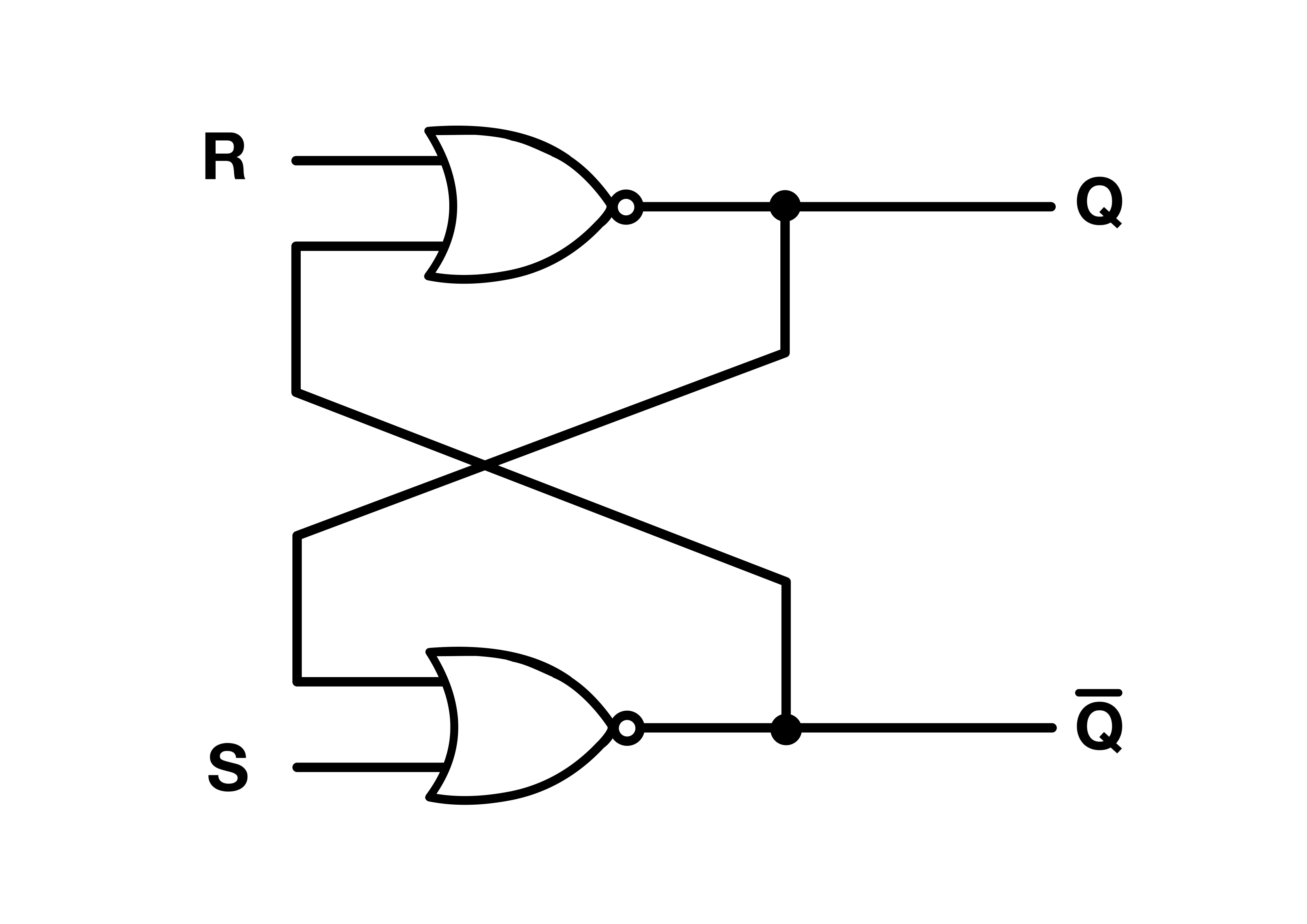

NOR SR Latch Truth Table:
| S | R | Q (Next State) | Q’ (Next State) |
|---|---|---|---|
| 0 | 0 | Q_prev | Q’_prev |
| 0 | 1 | 0 | 1 |
| 1 | 0 | 1 | 0 |
| 1 | 1 | ? | ? |
The behavior of the SR latch is as follows:
- When both S and R are 0, the latch retains its previous state.
- When S is 0 and R is 1, the latch is reset (Q becomes 0).
- When S is 1 and R is 0, the latch is set (Q becomes 1).
- The state when S and R are both 1 is typically considered an invalid or undefined state for an SR latch. You’d be telling the latch to set the value of Q to both 1 and 0 simultaneously.
The SR Latch can store a single bit of data and is used in various applications where simple storage and retrieval of a binary state are needed.
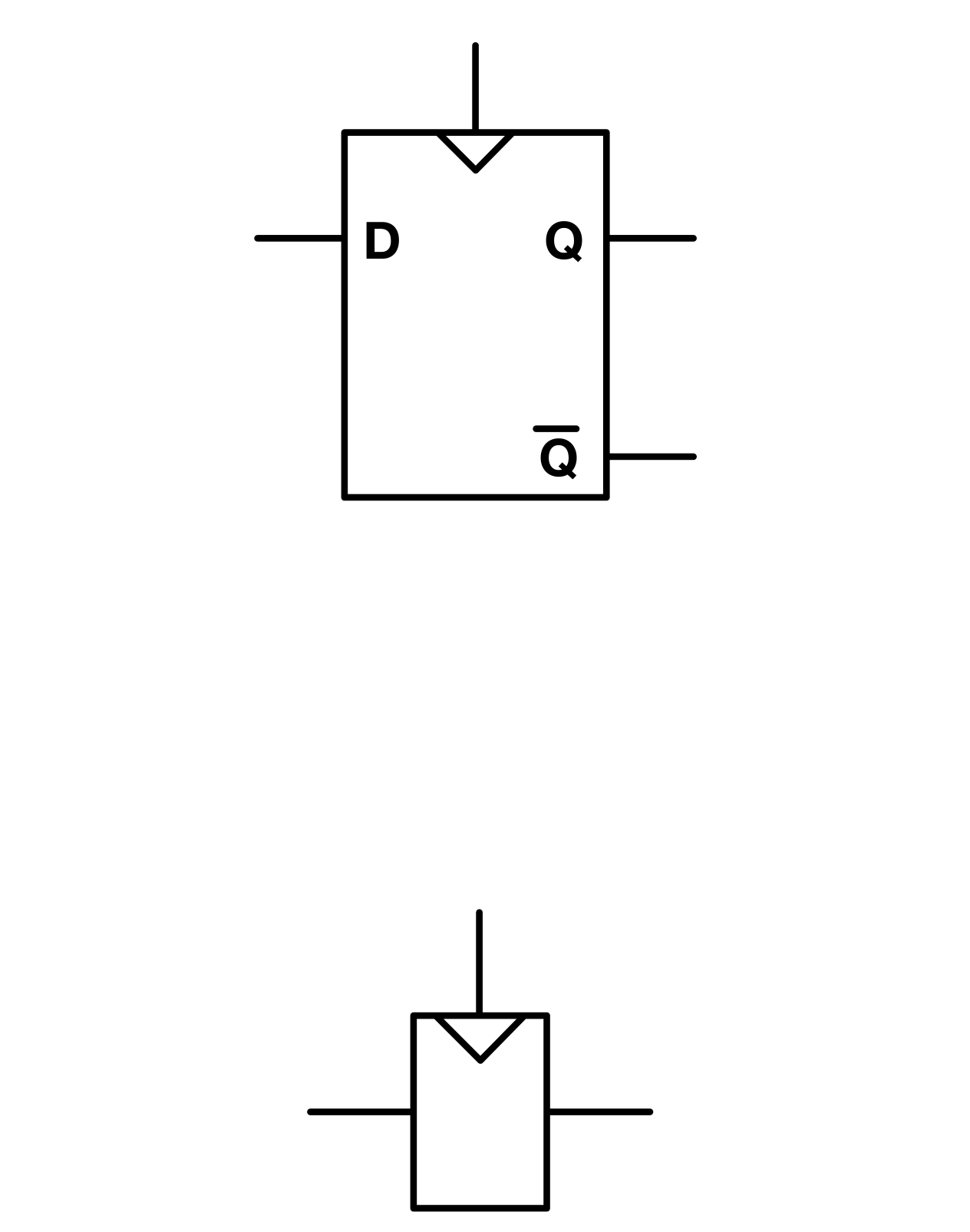
D Latch
The D (Data) Latch, also known as a transparent latch, is a more complex form of a latch with a single data input, labeled D. It also includes an enable input, often labeled E or CLK (clock). The D Latch captures the value at the D input only when the enable input is active.
- Data Capture: When the enable input is active, the value at the D input is passed to the output Q.
- Hold State: When the enable input is inactive, the latch retains the last value held at Q before the enable was deactivated.

Unlike the SR latch, which can exhibit unpredictable behavior when both S and R are asserted simultaneously, the D latch avoids this ambiguity by clearly defining the roles of its inputs. The data input decides the value to be stored, while the clock input indicates the timing for the change in state.

D Latch Truth Table:
| CLK | D | S | R | Q (Next State) | Q’ (Next State) |
|---|---|---|---|---|---|
| 0 | X | 0 | 0 | Q_prev | Q’_prev |
| 1 | 0 | 0 | 1 | 0 | 1 |
| 1 | 1 | 1 | 0 | 1 | 0 |
The S and R columns are derived from the D input as per the D latch operation:
- When CLK is 0, the D latch does not change its state, regardless of the D input.
- When CLK is 1 and D is 0, the latch is reset.
- When CLK is 1 and D is 1, the latch is set.
The D Latch effectively separates the control of state change (CLK) from the data being latched (D), thereby improving the design and functionality over the basic SR Latch.
Flip Flops
Flip Flops are a type of latch that can store one bit of data but are triggered by clock edges. They are fundamental in sequential logic, used in timing applications, and as basic storage elements in shift registers, counters, and data storage devices.
- Edge Triggered: Flip Flops change their output state at specific times, determined by the rising or falling edge of a clock signal.
- Types: Common types include the D Flip Flop (stores data from the D input on a clock edge), JK Flip Flop (more complex, with two inputs J and K), and T Flip Flop (toggles its state on a clock edge).
The D Flip Flop
The D flip-flop(Abbreviated as D flop) can be constructed from two D latches L1, and L2 arranged sequentially, commonly referred to as the master and the slave.
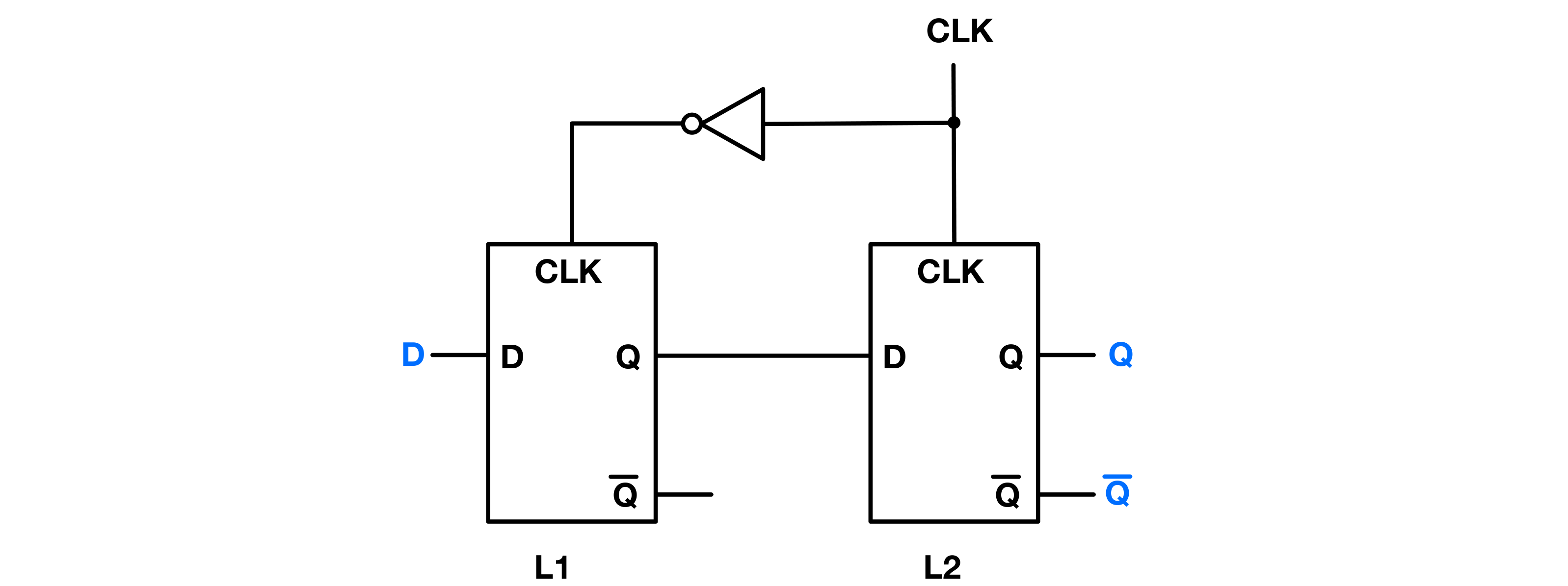
The working principle of a D flip-flop involves synchronizing these two latches with complementary clock signals:
- Master Latch (L1): When the clock signal CLK is at a LOW state (0), this latch is in a transparent state, allowing the data input D to pass through and be available at the output ($Q_{L1}$). During this phase, the slave latch is in an opaque state, not allowing changes to propagate to its output ($Q_{L2}$).
- Slave Latch (L2): As the clock signal transitions from LOW to HIGH (rising edge), the master latch becomes opaque, holding the data present at the transition moment. Simultaneously, the slave latch turns transparent, passing the value at ($Q_{L1}$) through to the output ($Q_{L2}$).
Generally any symbol with the triangular mark like the one on the flop’s top pin means that the device is clock-dependent(edge triggered).
The key functionality of a D flip-flop is its edge-triggered behavior. It updates its state (output Q) only at the rising edge of the clock signal and captures the data value present at the input D just before this transition. At all other times, the output Q maintains its previous state due to the configuration of the latches, effectively blocking any path between D and Q.
Registers
A register is a group of flip flops with a common clock input used together to store multiple bits of data.
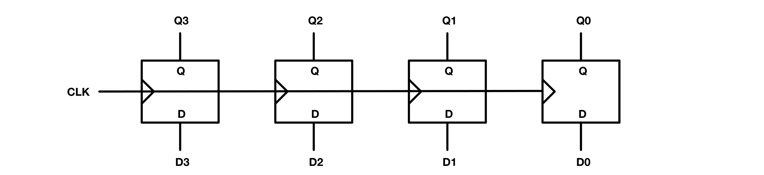
Registers can hold data temporarily during processing. For example, a CPU can uses registers to hold the current instruction, the location of the next instruction, intermediate results, and other data.

«««««««««« Previous Post: Nomenclatures & Notes
Next Post: Debugging Clock »»»»»»»»»»
Updated: