Program Counter & Stack Pointer
Basics Primer
The Program Counter (PC), sometimes called the Instruction Pointer or Instruction Address Register, is a special-purpose register that keeps track of where the next instruction should be fetched from memory. During normal execution, the CPU reads the instruction at the address stored in the PC, then advances the PC to point to the next instruction. Control-flow instructions such as jumps, branches, subroutine calls, and returns can overwrite the PC with a new address and allow programs to continue execution from a different location.
Another important special-purpose register is the Stack Pointer (SP). The Stack Pointer keeps track of the current top of the stack, a memory region commonly used for temporary data, return addresses, and subroutine state. When data is pushed onto the stack, the SP moves to reserve space for the new value. When data is popped from the stack, the SP moves back after the value has been recovered. The exact direction depends on the CPU design.
J-K Flip Flop
The SR flip-flop/latch has an invalid input state when S = R = 1.
The JK flip-flop eliminates this issue by introducing a new input state which triggers a toggle action when J = K = 1.
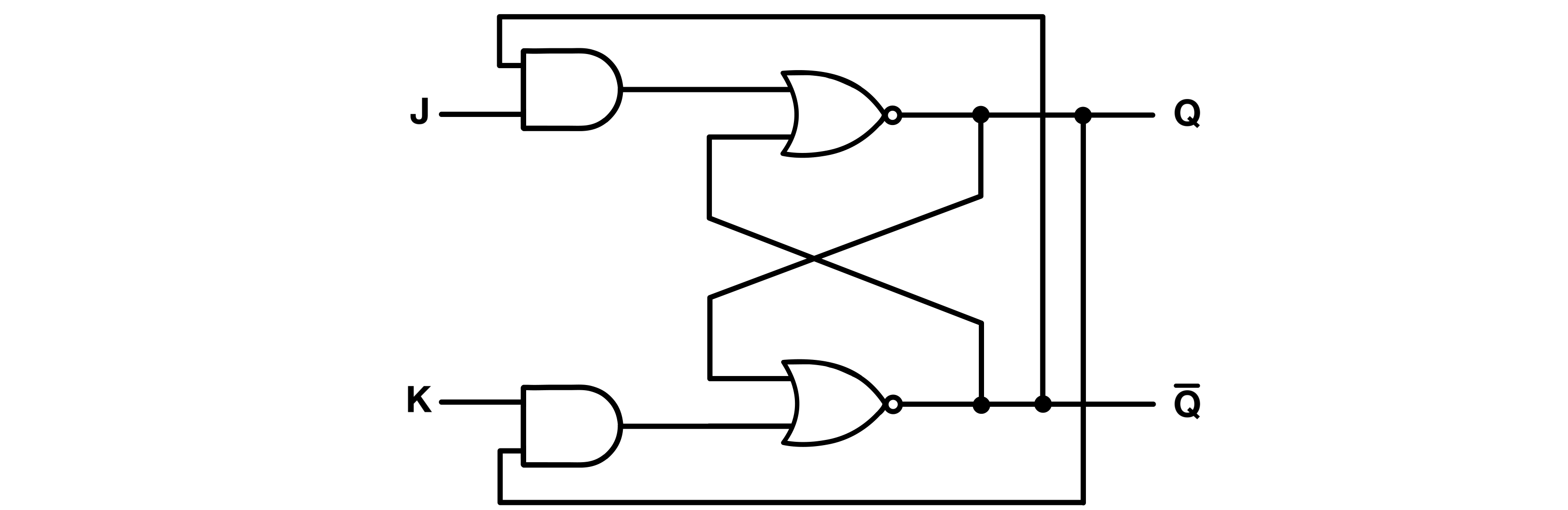
As can be seen from the schematic, the JK latch is actually an SR latch with its outputs cross-connected to its inputs using AND gates. These gates would never be HIGH/LOW at the same time, because Q and Q’ can never be HIGH/LOW simultaneously.
When J and K are both 1, the latch toggles (inverts its output values).
For example, let’s start with a set state in which Q = 1, Q’ = 0, and J = K = 0.
If J and K go HIGH at the same time ( J = K = 1), only the AND gate connecting J will go high, which will reset the SR latch (Q = 0 and Q’ = 1).
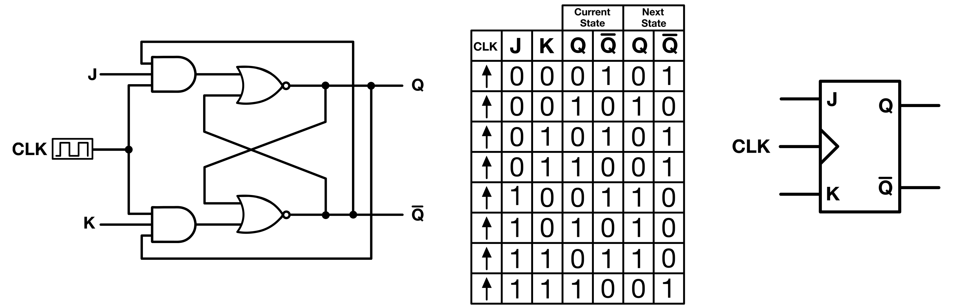
Adding a pulse detector to the JK latch turns it into a JK flip flop, as it now requires a clock for the AND gates to produce high outputs.
Binary Counter
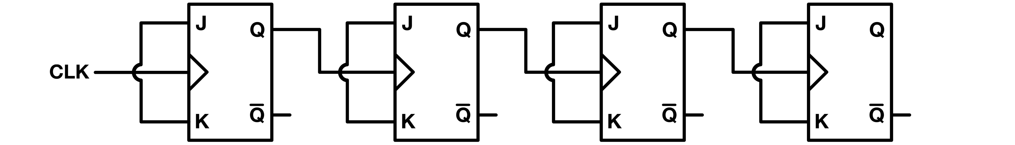
A binary counter is simply a sequential circuit that increments or decrements the value it holds at either a rising or falling edge of a clock.
A common circuit used to implement a counter is the JK flip-flop.
The implementation is very straightforward: simply cascade several toggled (J = K = 1) JK flip-flops (one per bit) that share the same clock. Naturally, this same methodology can divide a signal’s frequency.
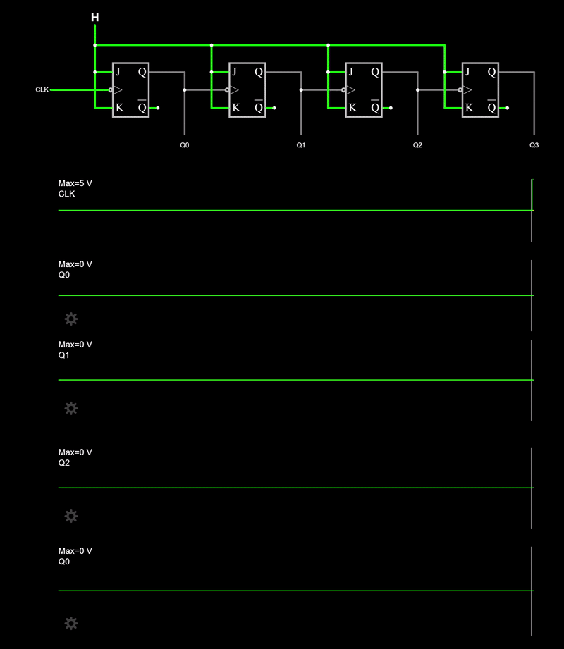
Below is a Falstad simulation of the circuit above:
Program Counter
The Program Counter (PC) typically increments its value sequentially. After the CPU fetches the byte or instruction at address “n”, the PC advances to address “n + 1”. However, control flow instructions such as jumps, branches, and calls can alter this sequential progression. These instructions can change the PC to an address other than “n + 1”. As a result, the CPU can skip over code, repeat sections of code, or jump to a different part of the program based on a condition or an explicit command. Loops, conditional execution, and function calls all rely on this behavior.
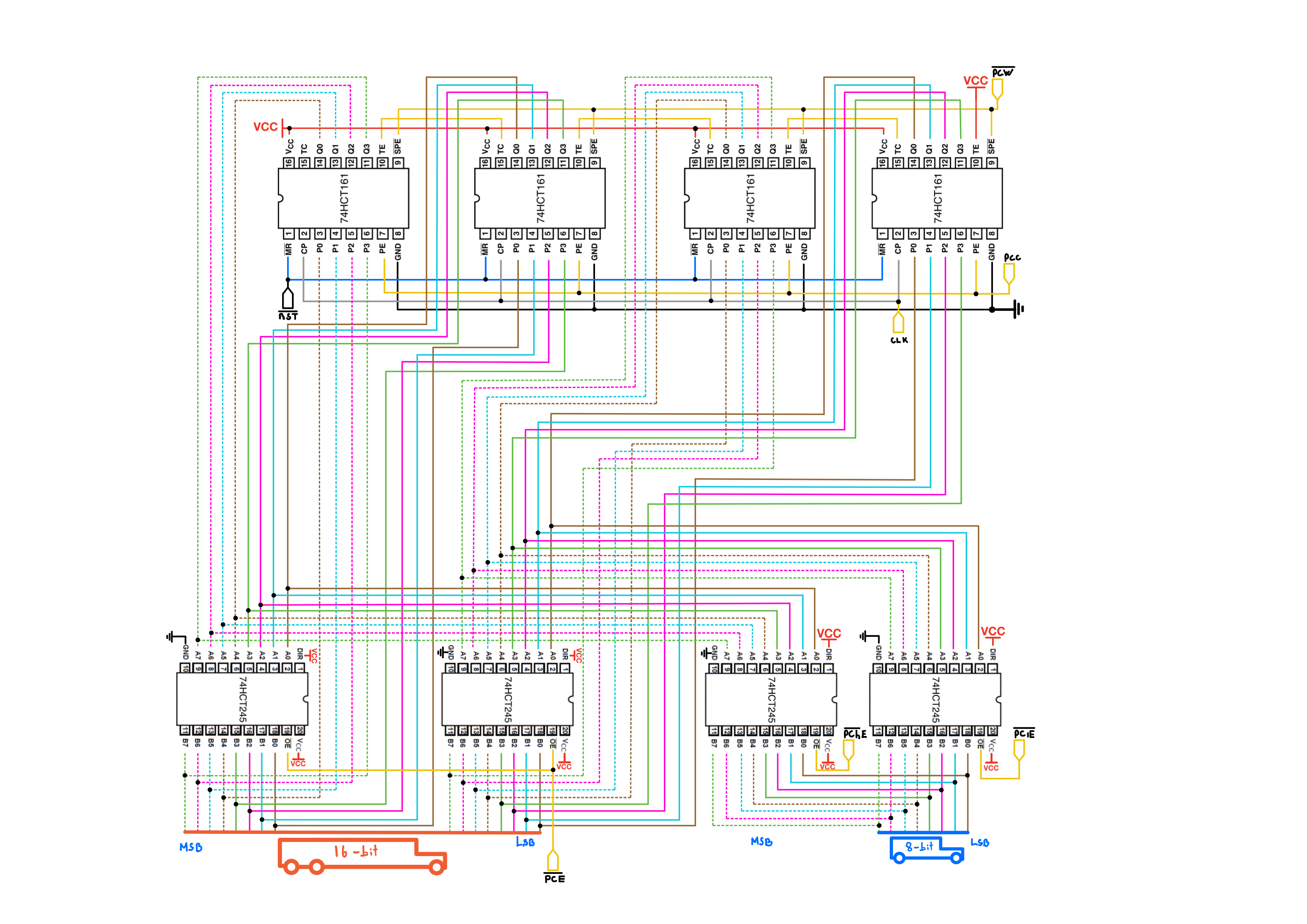
Since the CPU has a 16-bit memory bus, it naturally follows that the Program Counter should be 16-bit wide as well. The PC is made out of four cascaded 74HCT161 4-bit registers. Below are the schematic and pin descriptions of the chip.
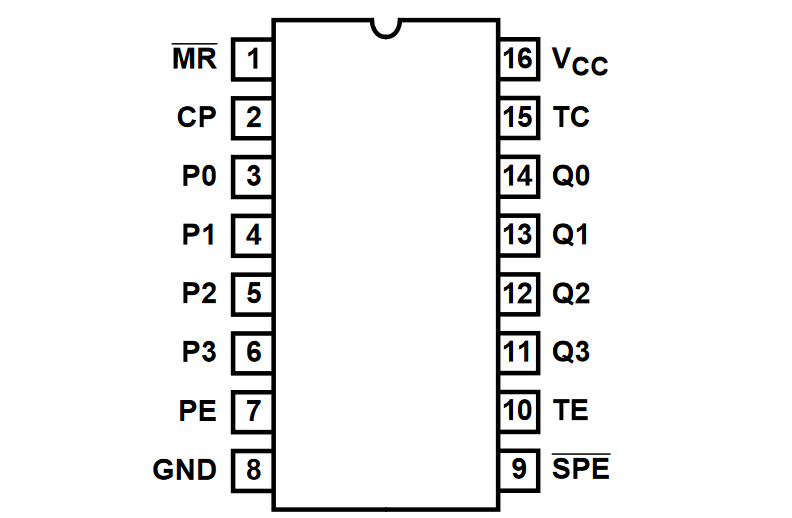
| Pin Number | Input Name | Description |
|---|---|---|
| 1 | ~MR | Clears the counters’ content when connected to Ground; inactive when connected to VCC |
| 2 | CP | Clock input |
| 3 to 6 | P0 to P3 | Parallel data inputs, used to load an arbitrary 4-bit value into the counter |
| 7 | PE | Enables(Counts up) all flip flops in parallel |
| 8 | GND | Ground |
| 9 | ~PE / ~LOAD | Synchronous parallel load input. When LOW, the value on P0 to P3 is loaded on the next rising clock edge |
| 10 | TE | Enables a carry input from another counter, used in cascade configurations |
| 11 to 14 | Q0 to Q3 | Counter’s output bits |
| 15 | RCO | Ripple Clock Output, for cascading counters |
| 16 | VCC | Positive supply voltage |
Table 1: 74HCT161 Pin Configuration
74HCT161 Counter Cascading
Consider two n-bit counters to be used as a single 2n-bit counter. At first, it may seem sufficient to feed the most significant output bit of the least significant counter(C0) to the clock input of the most significant counter(C1), but it becomes obvious why this wouldn’t work with a simulation:
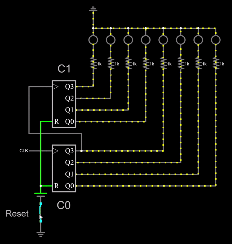
You can see that C1 increments its output every time the MSB of C0 rises, which is not desired. You want C1 to increment only when all the output bits of C0 are HIGH. In decimal, that would mean for example that all the 10s have incremented before starting incrementing the hundreds.
Here is a configuration which does exactly that. I connected a Falstad built-in 8-bit counter to the same clock as the cascaded counters to compare their outputs. The LEDs light up at approximately the same rate. I suppose the small delay comes from the circuitry of the built-in 8-bit counter.
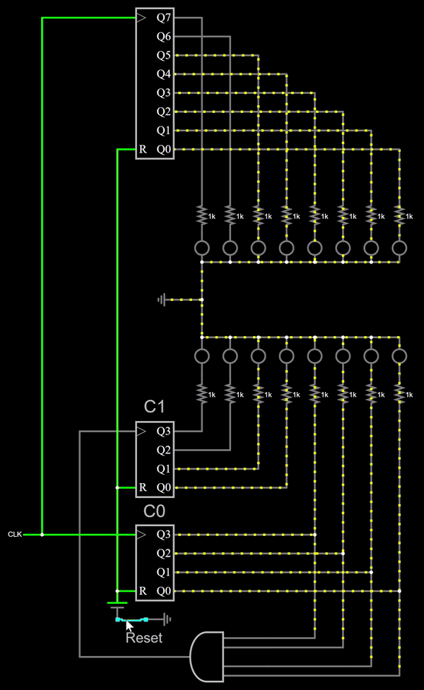
On the 74HCT161, RCO goes HIGH only when the carry-enable input and every counter output bit are HIGH. The Falstad simulation uses the same count-expansion principle, although its counters do not include ENT or ENP inputs.
In a nutshell, to operate two 74HCT161 counters, C0 and C1, in cascade: C0’s ENT can be permanently set to HIGH, while C1’s ENT can be connected to C0’s RCO.
Another important feature of the 74HCT161 is its asynchronous reset. It brings the PC to zero at CPU power-up, independent of the clock.
Stack Pointer
The Stack Pointer is also 16 bits wide because it drives the same 16-bit address space used by the rest of the memory modules. Even though the stack does not need the full 16-bit range in normal use, keeping the SP 16 bits wide lets it address memory directly without a separate narrowing circuit.
The stack itself is a section of memory used for temporary data. The Stack Pointer starts at 0xBFFF, which is the top of the lower 48 KB RAM region. This places the stack just below the bootloader ROM window, which begins at 0xC000.
In my CPU, the stack grows downward. A push operation writes the value to the memory address currently selected by the Stack Pointer, then decrements it afterward. A pull operation increments the Stack Pointer first, then reads the value from the new stack address. In other words, after a push, the Stack Pointer points one address below the most recently pushed value.
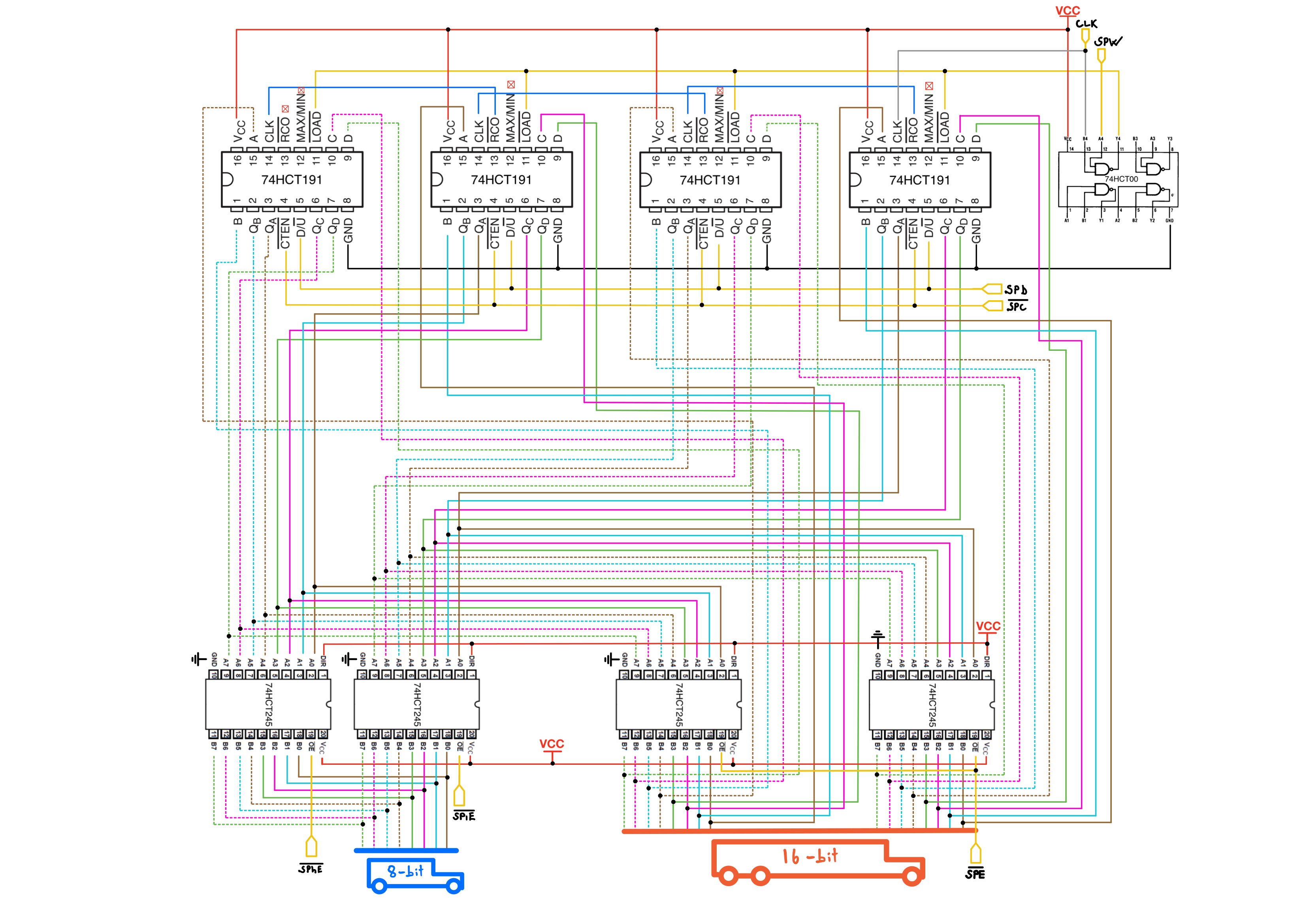
My stack pointer is implemented using four 74HCT191 up/down counters.

| Pin Number | Input Name | Description |
|---|---|---|
| 3, 2, 6, 7 | QA to QD | Counter’s output bits |
| 4 | ~CTEN | Enables(Counts up/down) all the flip flops |
| 5 | D/U | Down/Up direction input |
| 8 | GND | Ground |
| 11 | ~LOAD | Loads the counter when LOW; allows normal counting when HIGH |
| 12 | MAX/MIN | Terminal-count output. It goes HIGH when the counter reaches zero while counting down or reaches 15 while counting up |
| 13 | ~RCO | Ripple Clock Output, for cascading counters |
| 14 | CLK | Clock input |
| 15, 1, 10, 9 | D0 to D3 | Data input |
| 16 | VCC | Positive supply voltage |
Table 2: 74HCT191 Pin Configuration
Check out this nexperia datasheet for more detail on the 191.
As mentioned in the 191’s function table, ~CEN and U/D should only be changed during the HIGH phase of the clock. The 74HCT191 uses a direction input to select whether the counter counts up or down. In the standard CD74HCT191 convention, the counter counts down when D/U is HIGH and counts up when D/U is LOW. In my CPU, the direction control must be stable before the clock edge that performs the count. My schematic may label this control path according to the CPU-side signal name, so the important detail is the level that actually reaches the 74HCT191 D/U pin.
The 74HCT191 has an asynchronous load feature. This means the value on the counter’s input loads into the SP regardless of the clock’s state, as long as ~LOAD is LOW. Although this might not pose an issue in practice, I followed DerULF1’s guidance of NANDing the SPW (Stack Pointer Write) control line with the clock. This guarantees that the Stack Pointer updates during the HIGH phase of the clock.
Program Counter And Stack Pointer Working Principle
TThe Program Counter normally increments sequentially from one instruction address to the next, in the order the instructions are stored in memory. However, a “jump” instruction disrupts this sequential flow. A jump changes the PC to a different memory address. This lets the CPU skip over part of the code, repeat an earlier section, or continue from another location based on a condition or an explicit instruction. That changes the normal flow of execution because the CPU no longer continues with the next sequential instruction.
Unlike the Program Counter, the Stack Pointer can count both up and down. In this CPU, the stack grows downward: push operations write to the current stack address and then decrement the Stack Pointer, while pull operations increment the Stack Pointer first and then read from the new stack address. This convention means that after a push, the Stack Pointer points one address below the most recently stored value.
Example of PC and SP working principle
Immediate instructions (the ones that handle an arbitrary number directly) in my CPU require two memory locations: one for the microcode, and one for the number. For the sake of this example, let’s assume that all instructions take only one memory location.
Initial Conditions:
Let’s assume the following program is loaded into memory starting from address 0x0000:
MOV $A, 5

PSH $A

STC

SUB $A, 1

STC

CMP $A, 0

PUL $A

JZ 0x0200  ; Jump to address 0x0200 if the zero flag is set
; $PC points to the first instruction in memory at 0x0000
; The stack is empty. $SP points to 0xBFFF, the highest address used by the stack.

MOV $A, 5  ; Load 5 into register A.
; $PC now points to the next instruction (PSH $A at address 0x0001)
; $SP remains unchanged (still points to address 0xBFFF)

PSH $A ; Push the content of register A onto the stack
; $PC now points to the next instruction.
; The value from $A is written to the current stack address, 0xBFFF.
; $SP is then decremented to 0xBFFE.

STC       ; Prepare ordinary subtraction by setting carry/no-borrow.
SUB $A, 1 ; Subtract 1 from the value in register A. Now $A holds 4.
; $PC now points to the next instruction.
; $SP remains unchanged.

STC       ; Prepare ordinary compare by setting carry/no-borrow.
CMP $A, 0 ; Check if A is zero.
; $PC points to the next instruction.
; $SP remains unchanged.

PUL $A ; Pull the top value from the stack into register A
; $PC now points to the next instruction.
; $SP is incremented first, from 0xBFFE back to 0xBFFF.
; The CPU then reads the value at 0xBFFF into $A.

JZ 0x0200  ; Jump to 0x0200 if the previous CMP set the zero flag.
; Since CMP $A, 0 did not set the zero flag, execution continues after JZ.
; $SP remains unchanged (still points to address 0xBFFF)

; ... The code would continue with other instructions starting here

; Address to jump to if A was zero
0x0200:
; $PC would only have pointed here if $A was zero in the CMP instruction
; $SP would remain unchanged from its state before the jump
; ...This section would contain instructions specific to the case where A
; was zero.
Implementations
Program Counter
Control lines involved (5):
- |← ~PCW Program Counter Write(Jump)
- |← PCC Program Counter Count Up: Increments PC by 1
- |← ~PCE Program Counter word(16-bit) Enable
- |← ~PChE Program Counter upper/high byte enable Enable
- |← ~PClE Program Counter lower byte enable Enable
Below is the schematic of my PC module. The pair of 8-bit bus transceivers on the right enables writing either the upper or lower byte of the PC to the data bus with ~PChE and ~PClE respectively. The pair of transceivers on the left allows the counter to output its value to the 16-bit address bus in a single cycle with ~PCE. The PC can also be directly loaded from the address bus with ~PCW.
Stack Pointer
Control lines involved (6):
- |← SPW Stack Pointer Write / Load
- |← ~SPC Stack Pointer Count Enable: enables the Stack Pointer to count
- |← SPD Stack Pointer Count Direction: selects whether the Stack Pointer counts up or down
- |← ~SPE Stack Pointer word enable: allows the 16-bit Stack Pointer value to drive the address/system bus
- |← ~SPhE Stack Pointer upper/high byte enable Enable
- |← ~SPlE Stack Pointer lower byte enable Enable
Below is the schematic of the Stack Pointer module. The pair of 8-bit bus transceivers on the left enables outputting either the upper or lower byte of the Stack Pointer to the data bus with ~SPhE and ~SPlE, respectively. The pair of transceivers on the right allows the SP to output its value to the 16-bit address/system bus in a single cycle with ~SPE.
ICS
Program Counter
4x 74HCT161, Synchronous 4-Bit Binary Counters, (Digikey, Datasheet)
4x 74HCT245, Octal Bus Transceivers With 3-State Outputs, (Digikey, Datasheet)
Stack Pointer
4x 74HCT191 Synchronous Up/Down Counters with Down/Up Mode Control(Digikey, Datasheet)