
 Clock
Clock
 Memory
 Control
Debugging Clock
Basics Primer
Multivibrators
Multivibrators are digital oscillator circuits with two stable states. The transitions between the states can be controlled or automatic, and define the multivibrator’s behavior and application. The three forms of a multivibrator circuits are astable, monostable, and bistable.
Astable Multivibrator
An astable multivibrator has no stable state. It continually switches between two output levels and produces a repeating pulse signal, which makes it useful as a clock source in digital systems.
Monostable Multivibrator
The monostable multivibrator has one stable state. When triggered, it shifts to a quasi-stable(temporary) state for a predetermined period before returning to its stable state.
Bistable Multivibrator
The bistable multivibrator has two stable states. It changes from one state to another when triggered. A latch is a good example of a bistable multivibrator, as it maintains its output state either HIGH or LOW until it receives a trigger(Set or Reset) signal to change state.
The 555 Timer
Like the SAP-1, my CPU’s clock module uses a 555 timer. The 555 is a versatile chip that generates accurate pulses of various widths.
Compared to crystal oscillators, the 555 timer offers greater flexibility. Its circuitry makes it easy to manually adjust the clock speed. A crystal oscillator, as the name suggests, uses the mechanical resonance of a vibrating crystal to produce an electrical frequency. A single crystal oscillator is typically designed to generate a specific fundamental frequency determined by the physical properties of the crystal, such as its size, shape, and the way in which it is cut. It is possible for a crystal to support harmonics, which are integer multiples of its fundamental frequency. However, in the context of this breadboard CPU, the adaptability and control offered by the 555 timer are more convenient, especially for debugging and real-time modifications.
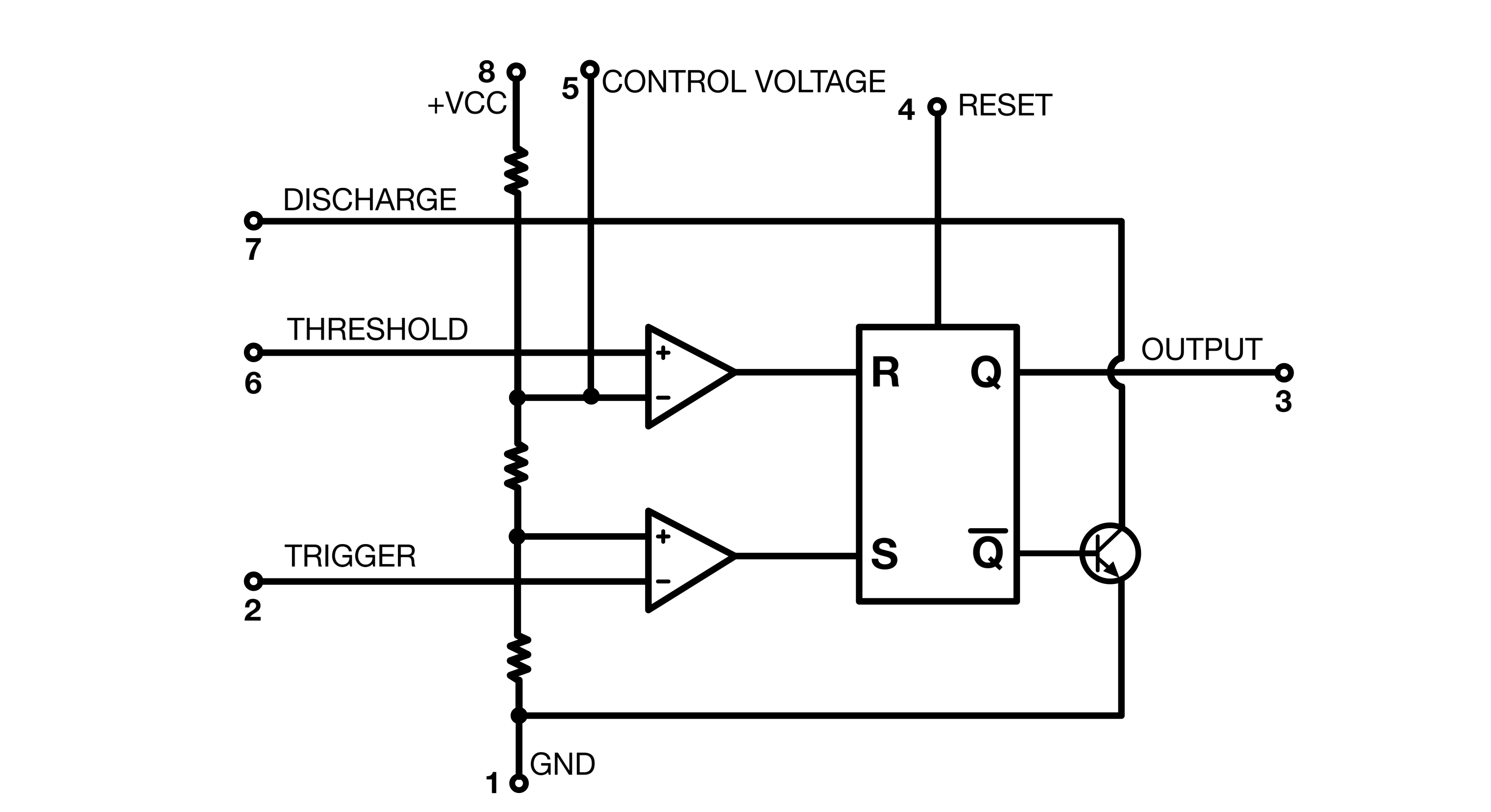
Below is a modularized schematic of the Texas Instruments LM_555 timer.
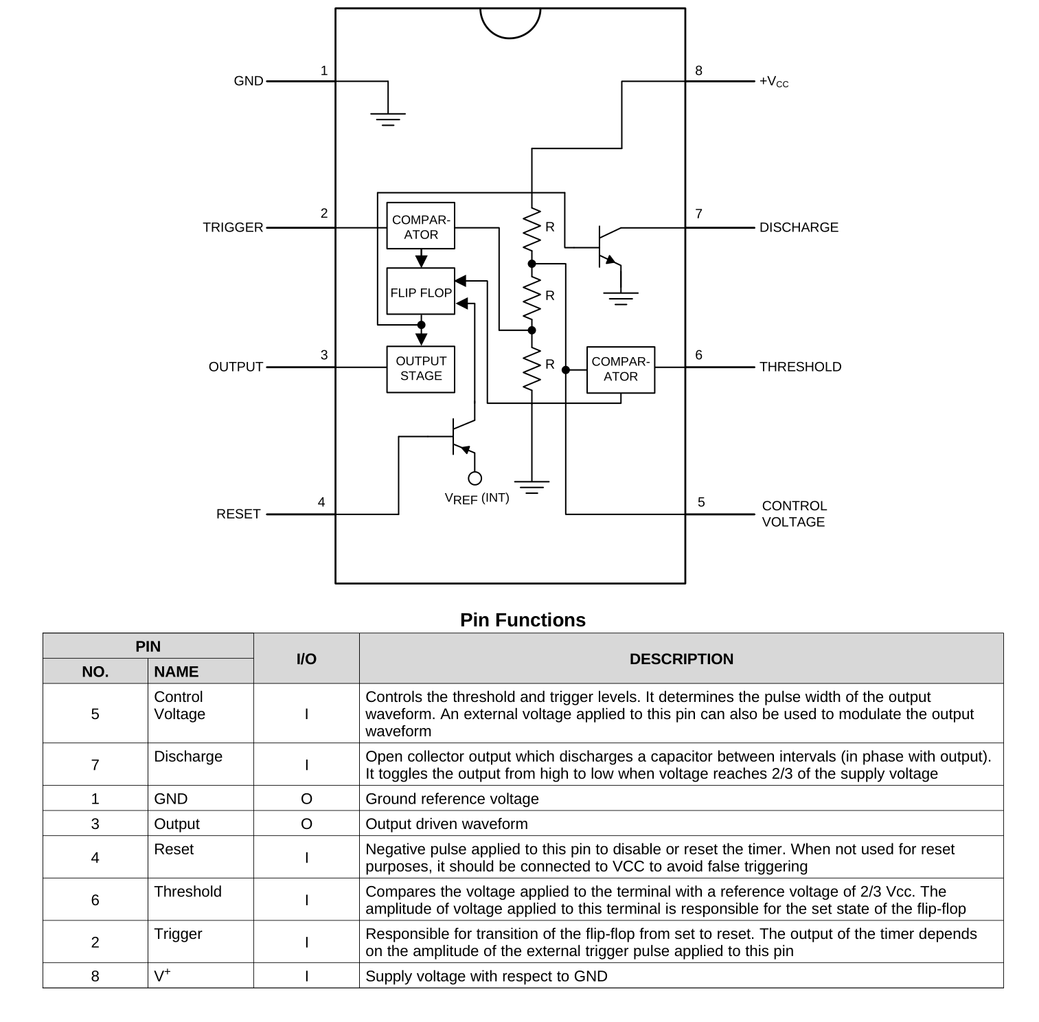
Three resistors in the center of the circuit form a voltage divider. The 555 timer got its name because the original model used three 5kΩ resistors.
Implementation
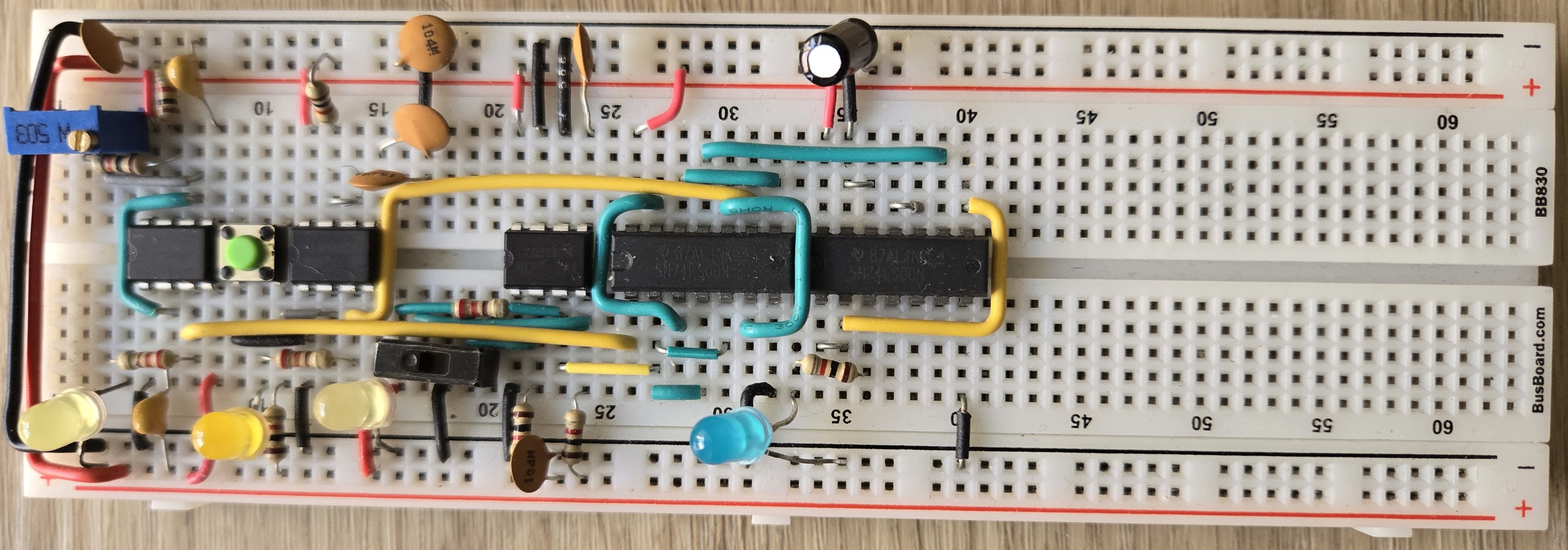
I’ve built two clocks for this project: a portable clock for debugging and a permanent clock for ongoing use. The permanent clock is described in the next post.
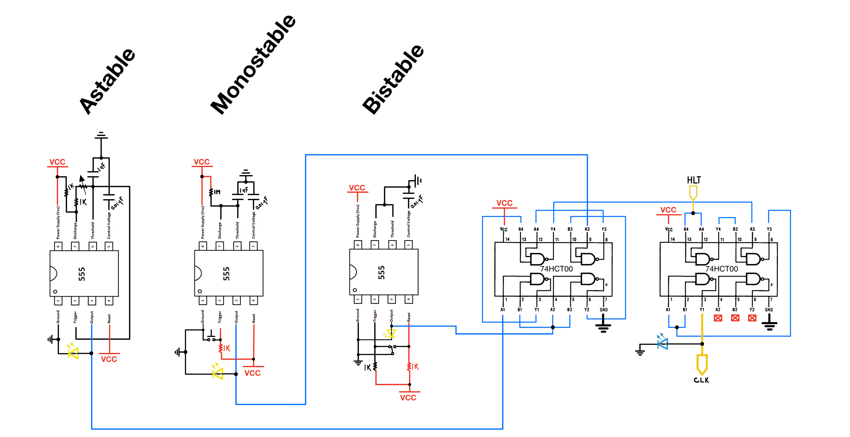
The debugging clock is similar to the SAP-1’s. It has an astable and a monostable configuration, selected with a switch for different testing needs.
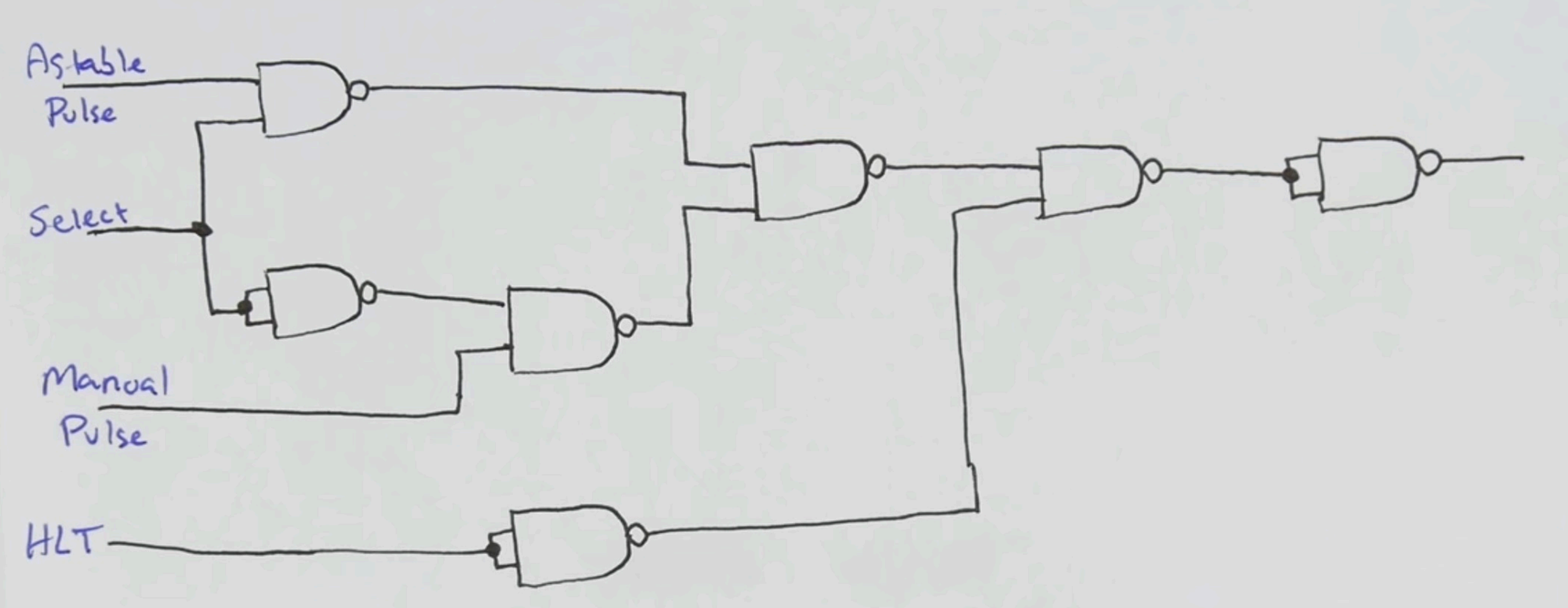
The difference between my clock and the SAP-1’s is the use of NAND logic for the astable-monostable output switching instead of AND logic.
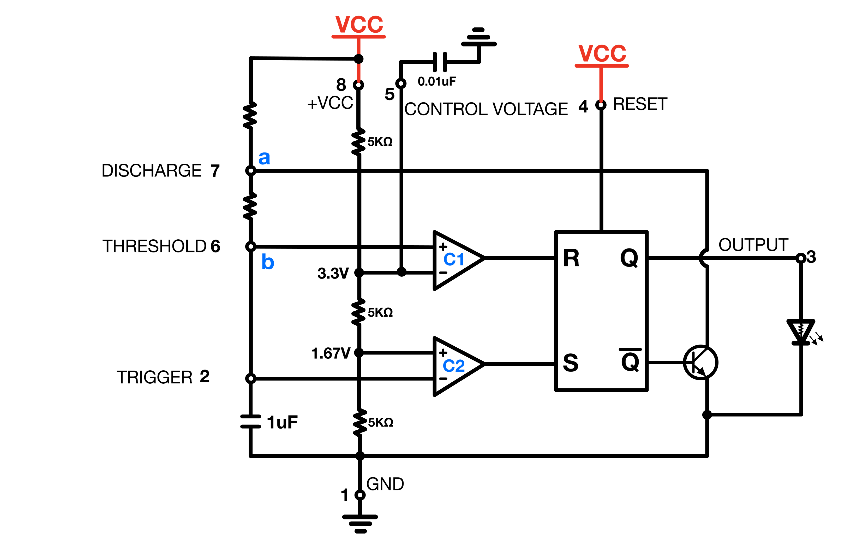
The simplified diagram of the 555 timer that Ben Eater used in his videos, shown below, is very helpful for building an intuitive sense of how the timer works.
Astable Multivibrator with 555
1. Initial Conditions
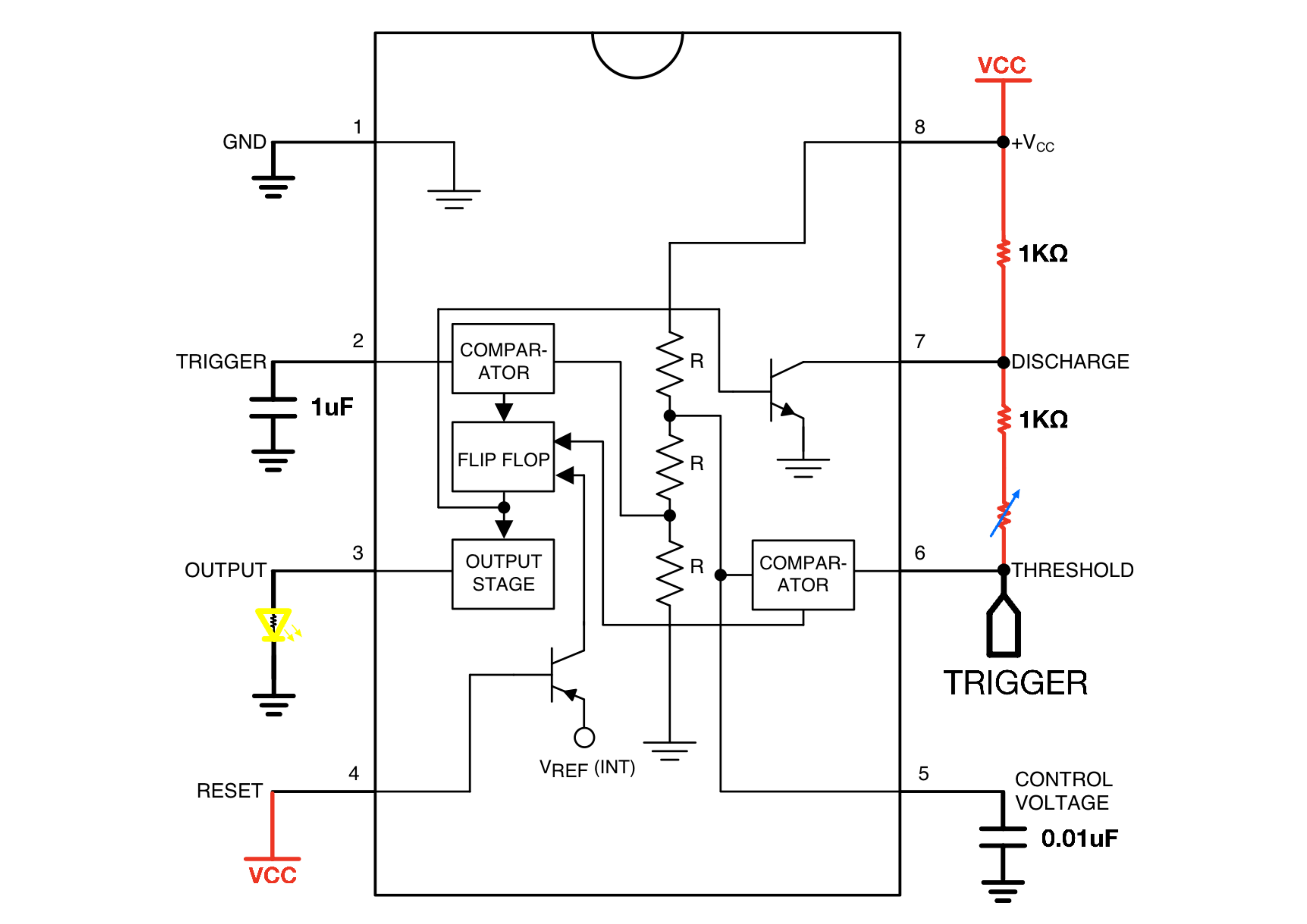
Upon powering up, assume nodes a and b (in the figure below) start at 0V. No matter how fast the capacitor at node b charges, the voltage divider’s node on the C2 comparator reaches 1.67V before node a reaches 1.67V. C2 stays ON until the voltage at node b surpasses 1.67V.
While C2 is ON, the latch’s “set” input stays ON, which keeps its “not” output OFF. As a result, the transistor connected to the discharge pin, (pin 7/node a) turns OFF. disconnects the path to ground and charges the external capacitor through the leftmost resistors.
2. Capacitor Charging
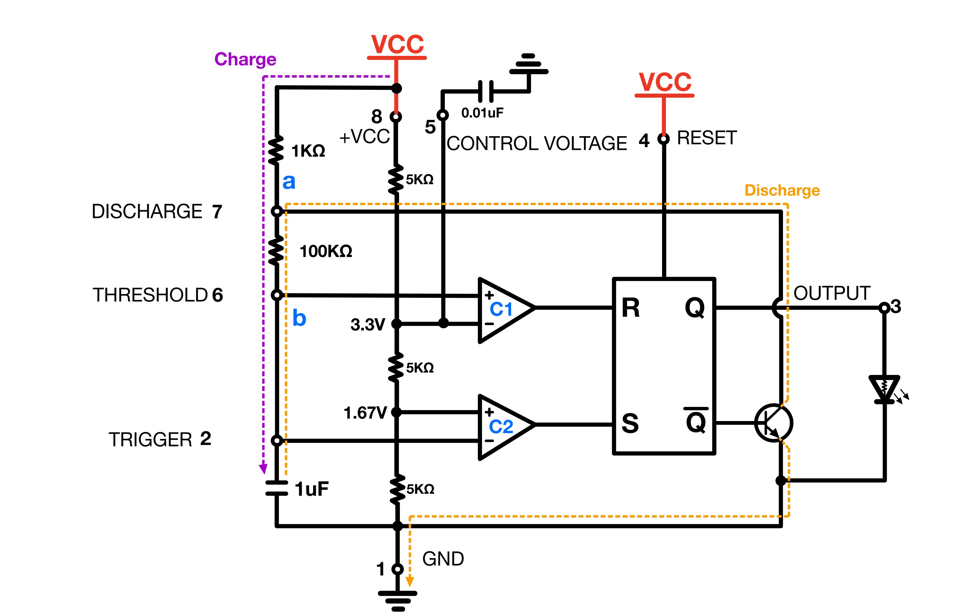
The external capacitor starts charging through the resistors. Current flows, and the voltage across the capacitor rises exponentially, following the RC charging curve.
As the capacitor charges, the voltage at node b eventually exceeds 1.67V. C2’s output goes LOW because the inverting input’s voltage is higher than the non-inverting input’s. The latch’s state remains unaffected.
2.1 Latch Reset
The capacitor charges until the voltage at node b surpasses 3.3V. At this point, the latch’s “reset” input gets activated because C1’s output turns HIGH (as the non-inverting input connected to node b is now higher than the inverting input). The latch’s “not” output goes HIGH, which turns ON the transistor.
2.2 Capacitor Discharging
With the transistor ON, the capacitor discharges through the timer’s discharge pin, and drops the voltage at node b. When it falls below 1.67V, C2’s output goes HIGH again, which sets the latch and turns the transistor OFF.
The cycle repeats, and produces a square-wave output at pin 3. The capacitor’s charging and discharging times define this wave. Varying these component values adjusts the oscillation frequency and duty cycle (the proportion of the cycle when the signal is HIGH).
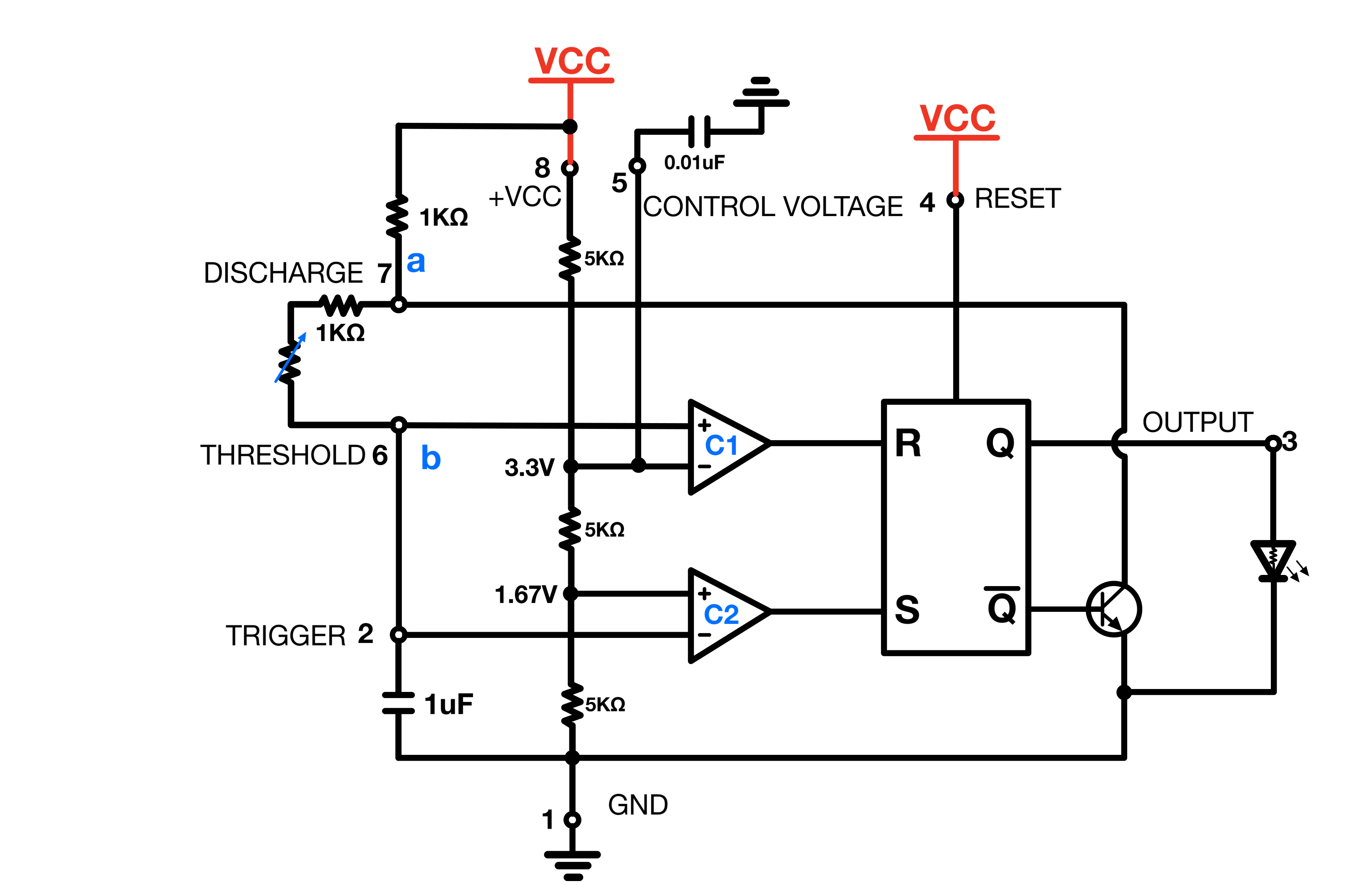
Typically, to have flexibility on the clock rate, a variable resistor is added in addition to a resistor between nodes a and b. The variable resistor alters the time it takes for the capacitor to charge and discharge, which changes the clock rate.
The 1KΩ resistor in series with the variable resistor is there so that in the event that the variable resistor is set to 0Ω, there would still be some resistance between pin 6 and pin 7, otherwise the discharge time would theoretically be zero(The capacitor would immediately discharge every time the voltage at node b hits 3.3V), which would keep the timer’s output constantly ON.
Let RA be the resistance between the voltage supply and the discharge pin and RB the resistance between the discharge and the threshold pin.
The charging time for the capacitor exceeds the discharging time, because the capacitor charges through both RA and RB, but only discharges through RB. As a result, the duty cycle exceeds 50%, with the exact excess percentage depending on the value of RA(The higher the value of RA, the further above 50% the duty cycle will be, and vice versa.)
The datasheet provides the following timing equations:
$t1$ = $0.693 (R_A + R_B) C$
$t2$ = $0.693 (R_B) C$
$T = t1 + t2 = 0.693 (R_A +2R_B) C$
$==> f =1/T=1.44/((R_A + 2R_B)C)$
Achieving a precise 50% duty cycle isn’t feasible in this setup without modifications. A zero-ohm Ra would technically yield a 50% duty cycle, but it’s impractical as it would create a direct short from VCC to ground via the discharge pin (pin 7).
However, as discussed in the permanent clock’s post, adding a (or a combination of) bypass diode(s) between pin 7 and pin 6 can allow duty cycles of 50% and below. The slightly imbalanced duty cycle resulting from the absence of such a modification is more than acceptable for the debugging clock.
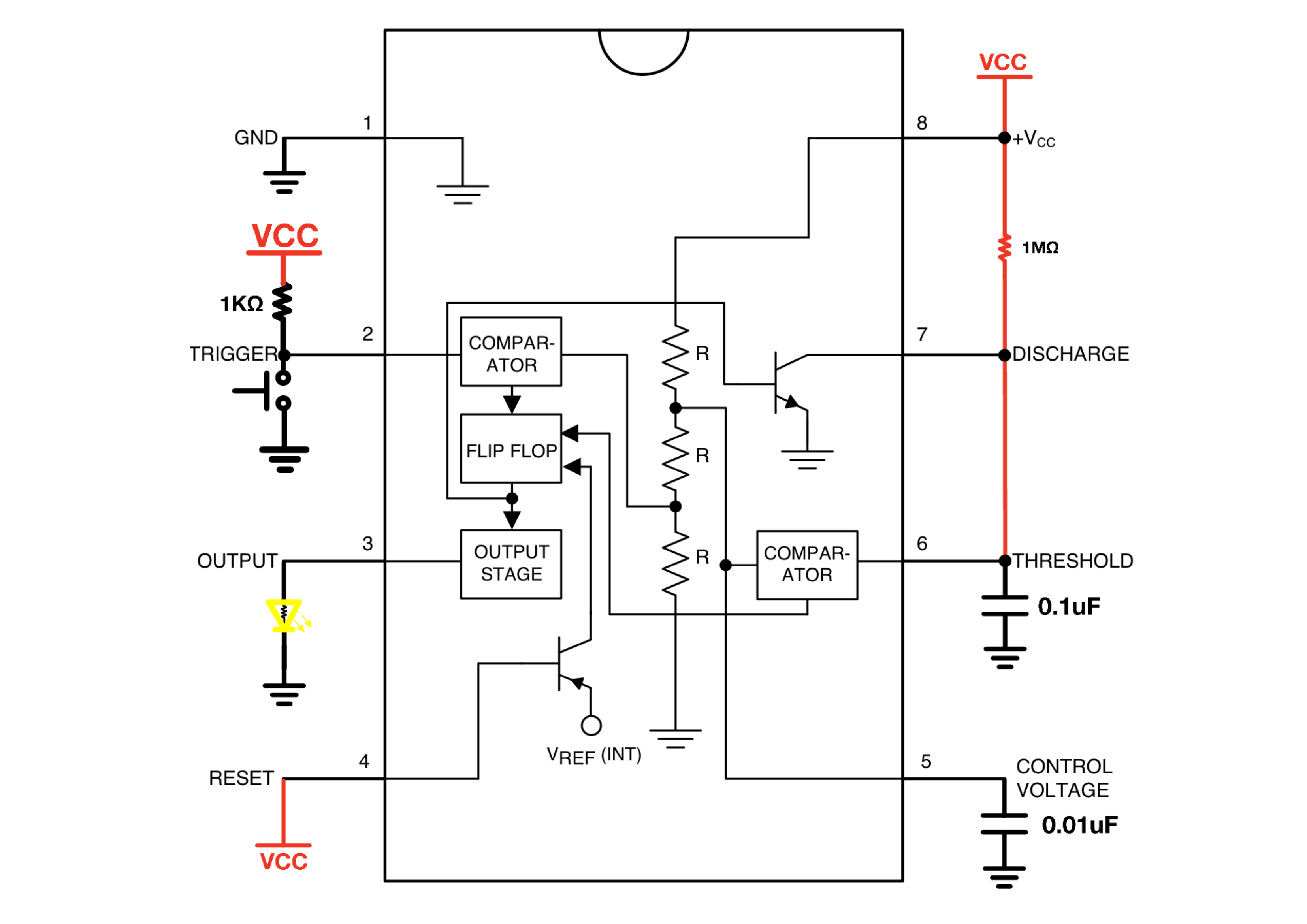
The 555 datasheet suggests adding a 10nf capacitor between pin 5 and ground, to reduce noise. Pin 5 is directly connected to the top node of the voltage divider and therefore sets the reference voltage for the comparator. Attaching a bypass capacitor to this pin helps keep the voltage level steady, and makes the timer more reliable.
Monostable Multivibrator with 555
The astable output lets the debugging clock run the CPU continuously, similar to a normal system clock. However, the point of a debugging clock is to mainly allow single, manual pulses.
A push button, by itself, can be used to tie the reference voltage to the clock node/input of the CPU. The problem here is that when pressing the button, its switch can unexpectedly close and open more times than intended. Just like in wristwatches with clicky buttons,one button press can sometimes advance the displayed time by several steps because the button’s internal contacts bounce.
To solve the problem, the 555 timer is used in a monostable configuration. A trigger makes the output change state for a set period before it returns to its original state. During that period, the output remains fixed regardless of the trigger signal. As a result, each button press produces a single clean clock cycle, even if the button bounces.
Working Principle
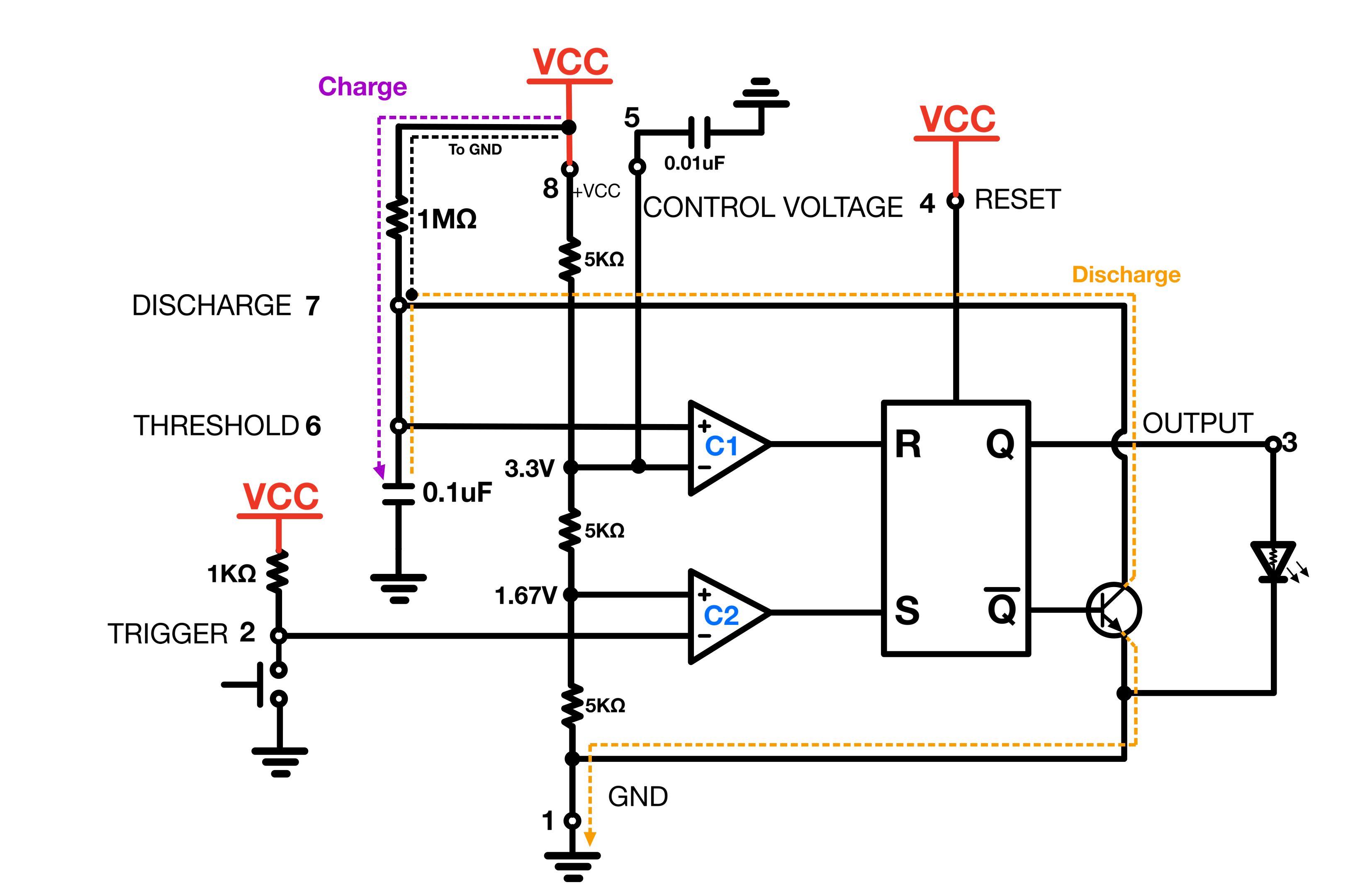
When the push button is not pressed, C2 stays OFF because pin 2 remains at the reference voltage through the 1 kΩ pull-up resistor. The latch stays in its reset state with the “not” output HIGH, so the transistor turns ON and discharges the capacitor.
Upon pressing the button, pin 2 gets connected to ground, and activates C2. With C2 ON, the output goes HIGH, the transistor turns OFF, and initializes the capacitor’s charging process.
The cycle resets when the capacitor’s voltage exceeds 3.3 V. At that point, C1 turns ON and resets the latch.
This turns the transistor ON and restarts the cycle.
This mechanism helps each button press produce one clean clock pulse despite mechanical bounce.
Bistable 555 Debouncer and Switching Logic
Bistable Debouncer
Just as a push button could have been used by itself to trigger clock pulses, a simple single-pole-double-throw (SPDT) switch can be used to switch between the two multivibrators outputs, as follows:

But just like push buttons, switches can also bounce. My switch, just like the one in the original SAP-1 kit, is a Break-Before-Make(BBM) switch.
The image below shows what’d happen within a SPDT BBM switch if used as shown above.
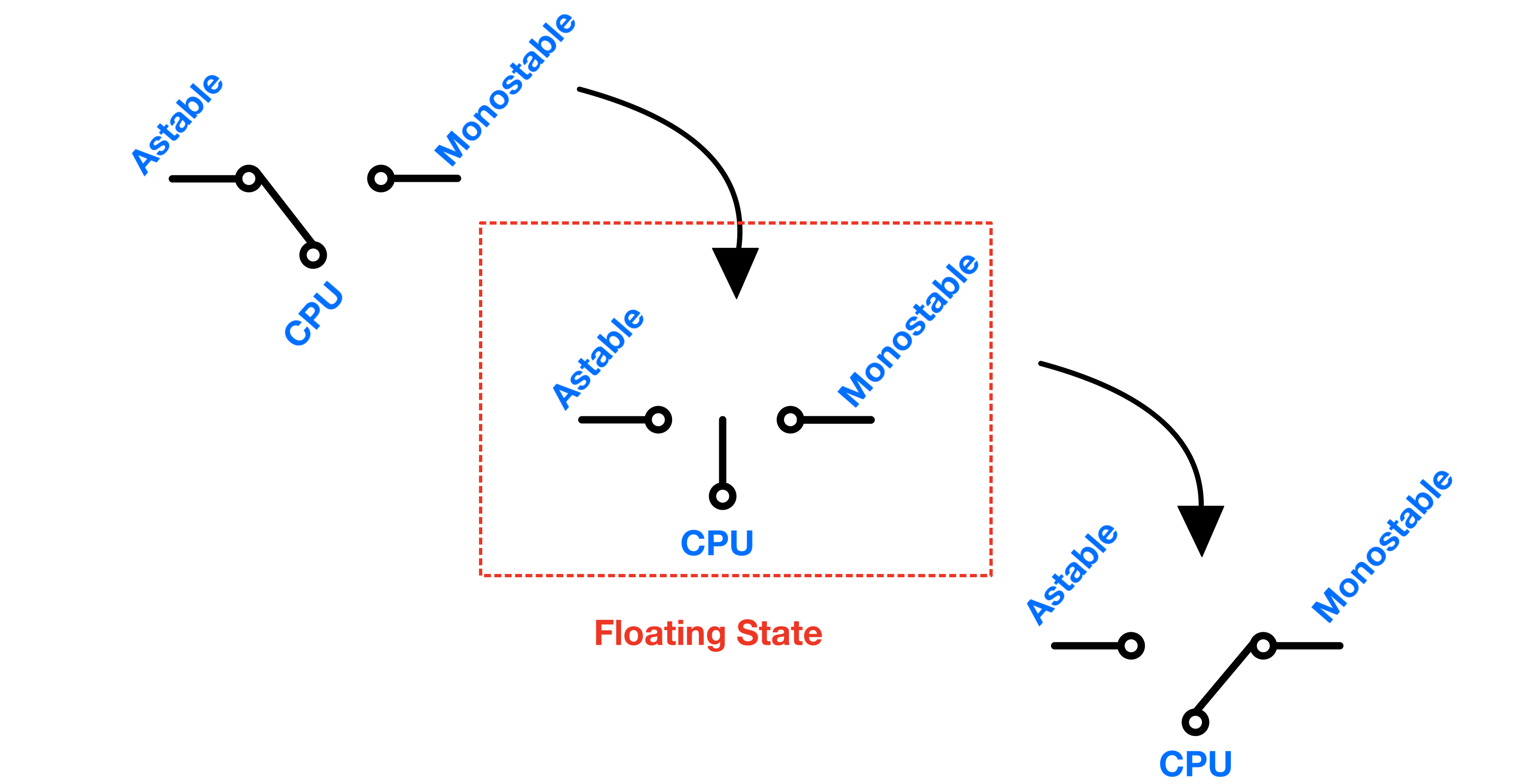
The pole within the switch can bounce with the last throw it made contact with due to slight vibrations, and all of the CLK input pins within the CPU would be momentarily left in a floating state during the switching process.
As mentioned earlier in this post, an SR latch is a bistable multivibrator by definition, and its output can be used with the switch through a switch-select logic to select(more so than switch) between the astable and monostable clock.
Ben Eater used a bistable configuration of the 555 timer to implement this debouncer just to expose learners to another use of the chip. The only component of the 555 timer used here is its SR latch, and in fact, an SR latch IC could have been used by itself.
I initially used the 555 to save space on the breadboard. Since I originally intended to use the debugging clock as the main clock, I wanted to pack as many ICs onto the board as possible.
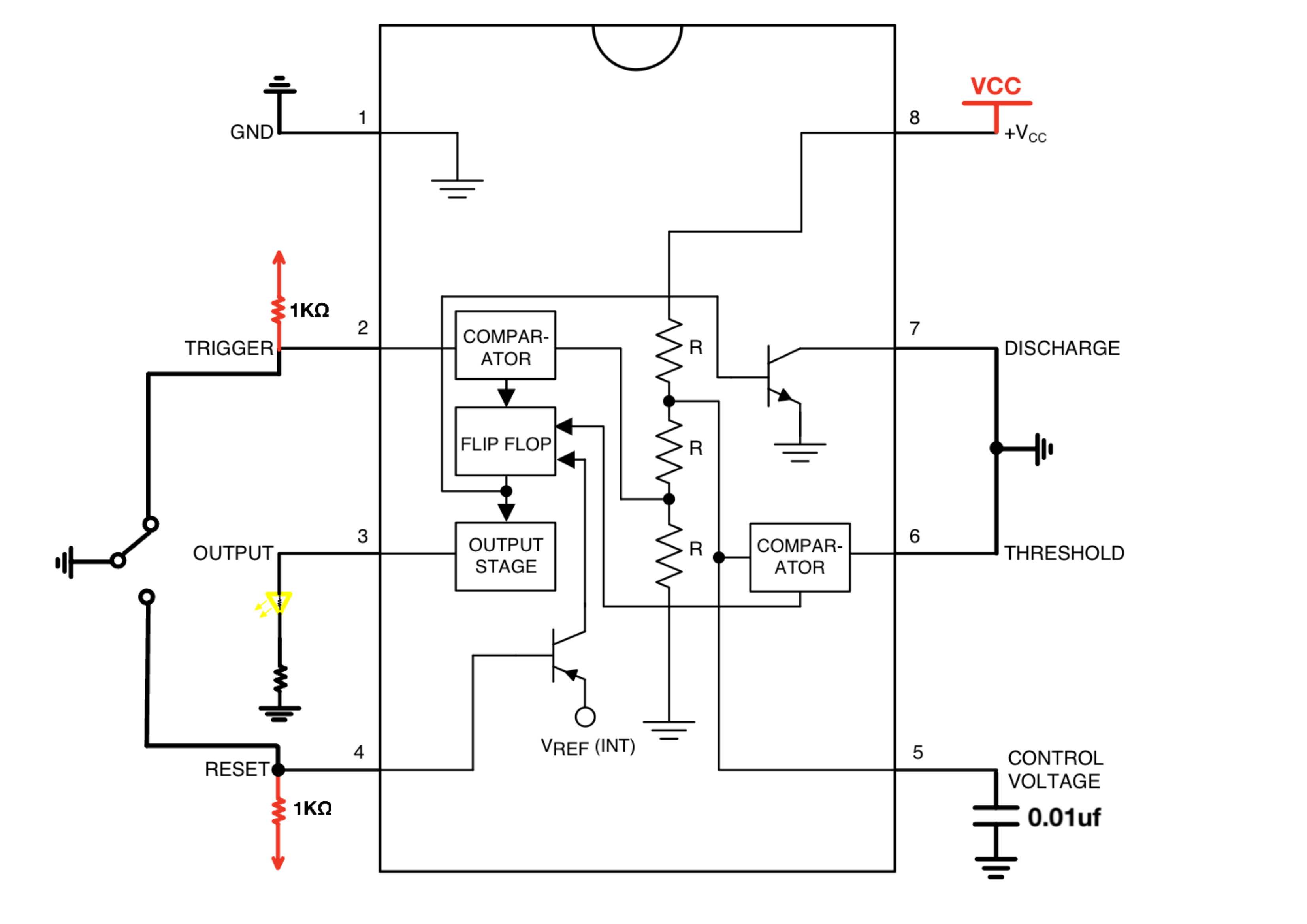
With this configuration, bouncing between a closed contact and a floating state does not change the latch’s output. The latch holds its current state until the switch reaches the opposite contact.
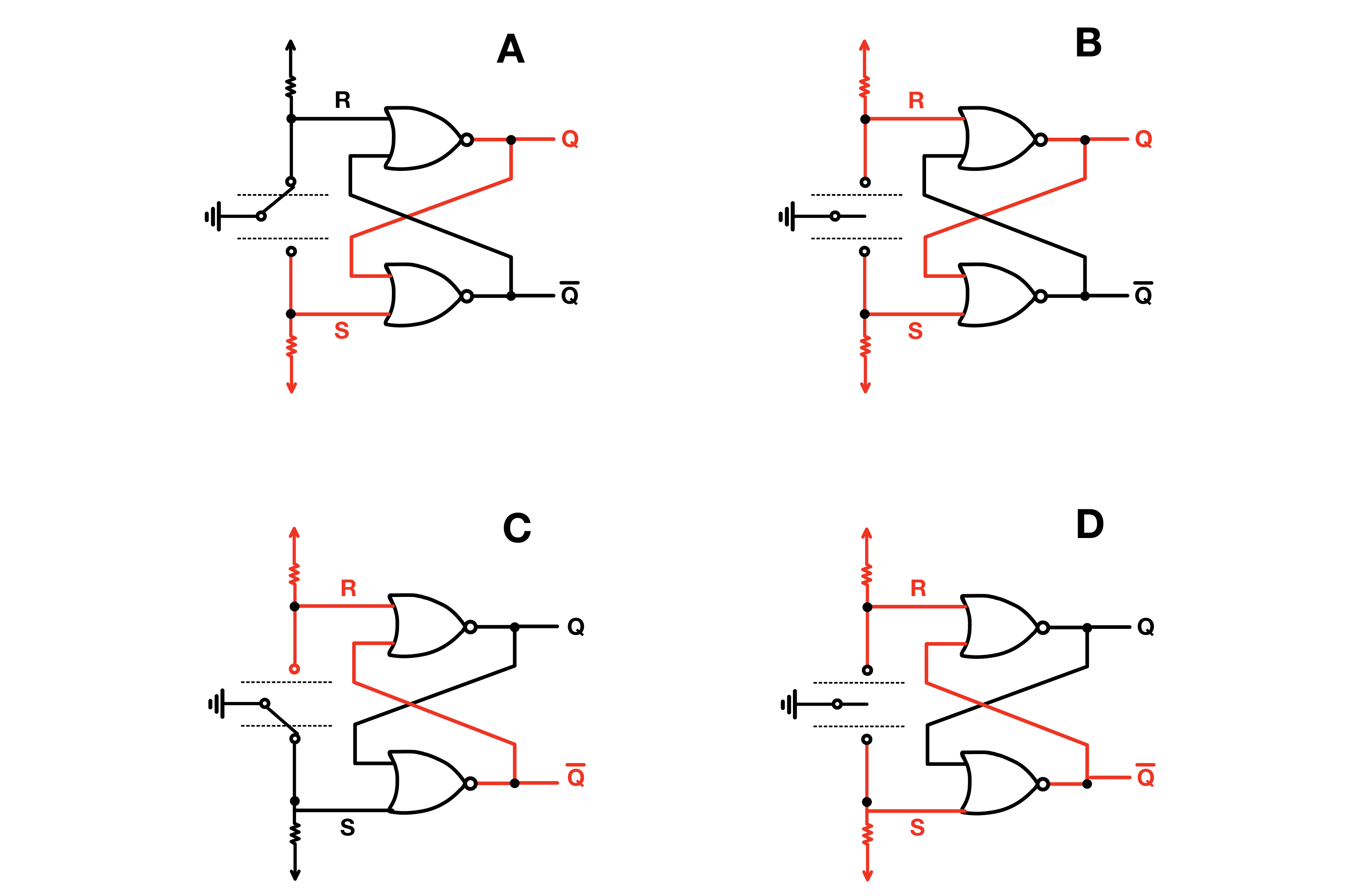
In other words, unless the opposite input (Trigger or Reset) is grounded, which does not happen until the switch is fully actuated, the output of the latch is not going to change even if the current input is being toggled!
Switching Logic
Once the astable, monostable, and bistable sections are complete, their outputs must be combined into one clock signal. The goal is to have a select input, tied to the bistable output, to switch between the astable and monostable pulses.
The logic below follows the approach used in the original kit.
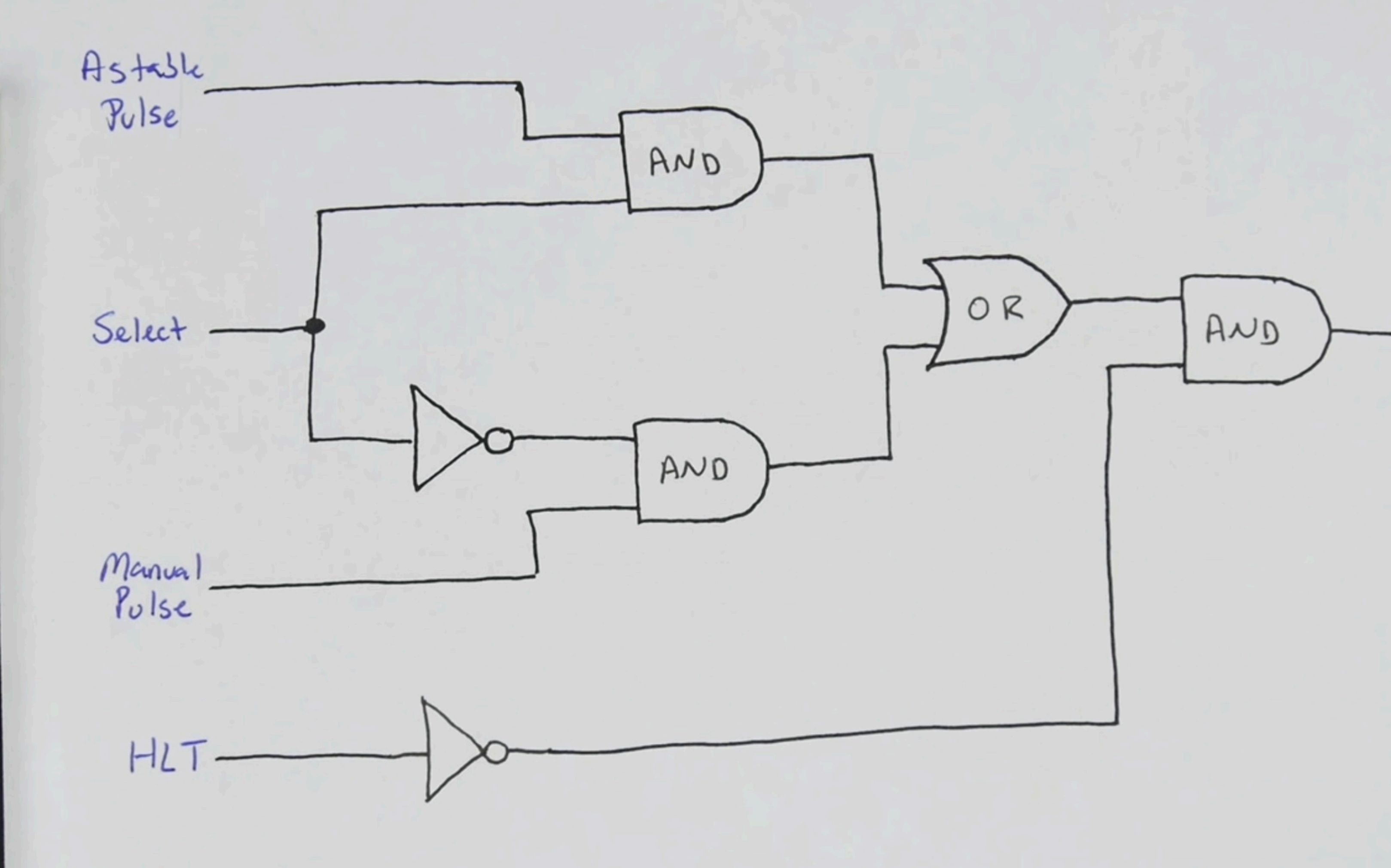
To save breadboard space, I implemented this logic using NAND gates. It requires only two ICs instead of the four shown above.
ICs
3x LMC555CN CMOS Single 555 Timer Low Power DIP-8 (Jameco, Datasheet)
2x 74HCT00 QUAD 2-INPUT POSITIVE NAND GATE (Jameco, Datasheet)