Permanent Clock
The debugging clock is useful for stepping through the CPU manually, but it is limited to relatively low frequencies. For normal operation, I wanted a dedicated clock that could run the CPU faster while still giving me control over the clock speed.
The permanent clock module generates the main CPU clock and uses a 4-bit register on the data bus to select one of eight clock rates. Assembly routines can write to that register when a lower speed is useful, for example during OLED animations or other timing-sensitive output.
Clock Speed Calculation
Propagation Delays and Critical Path
Propagation Delay
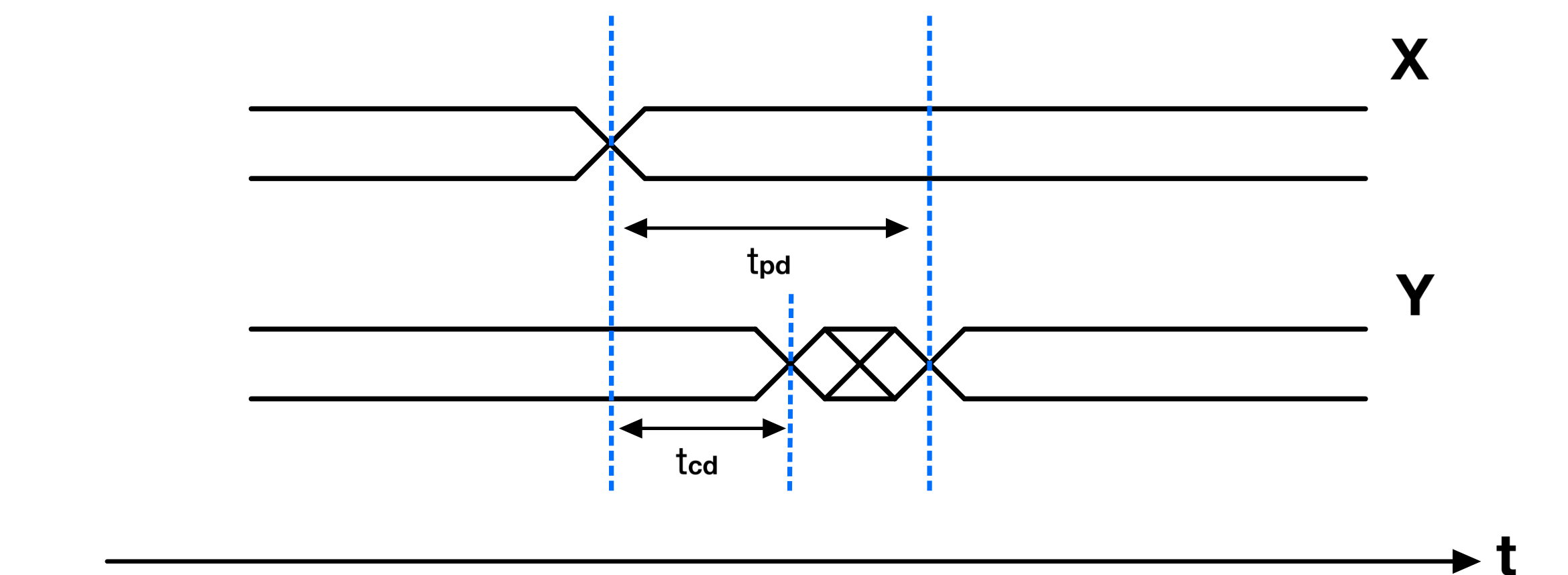
The propagation delay ($t_{pd}$) of a digital circuit is the maximum time taken for a change in input to stably reflect at the output. Different kinds of propagation delays arise due to the inherent physical characteristics of the circuit components, such as the capacitive and resistive properties of transistors and the interconnections between them. They vary from component to component and are influenced by factors like temperature, supply voltage, and manufacturing variances.
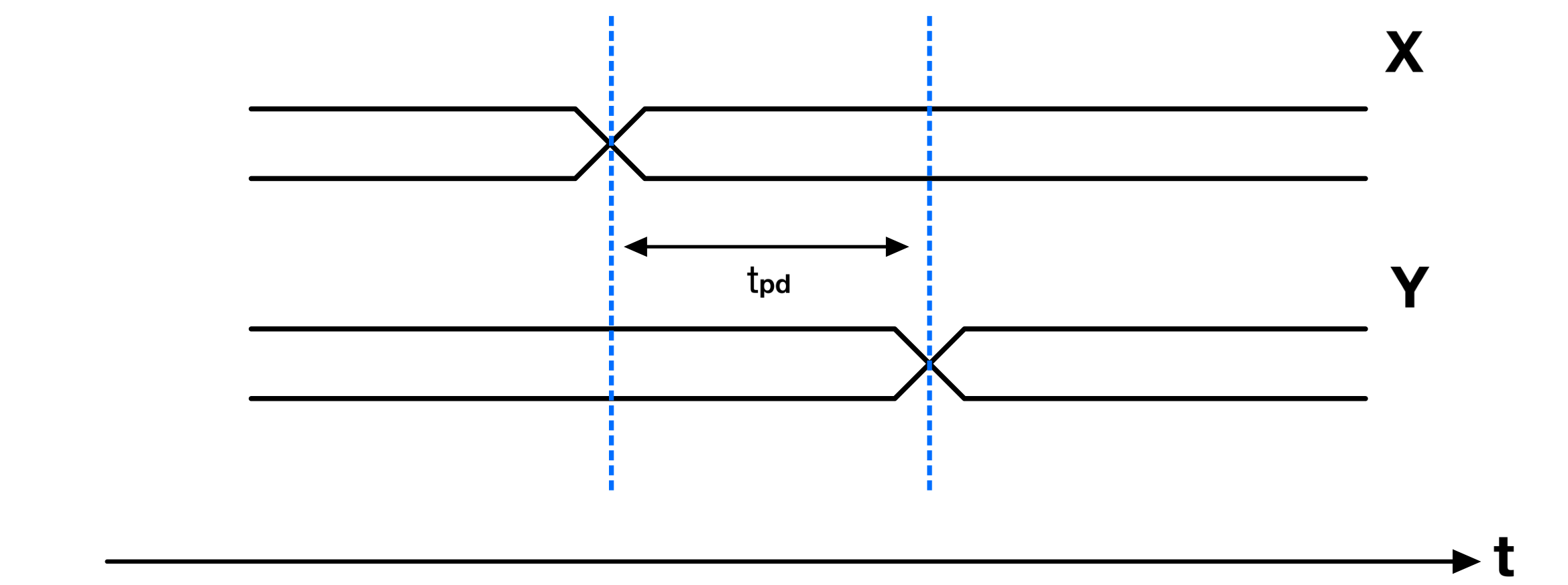
There is also a related timing parameter called contamination delay, which describes the minimum time before an input change can begin to affect the output. For this post, I focus on the maximum propagation delays because they are the limiting factor for the highest safe clock speed.
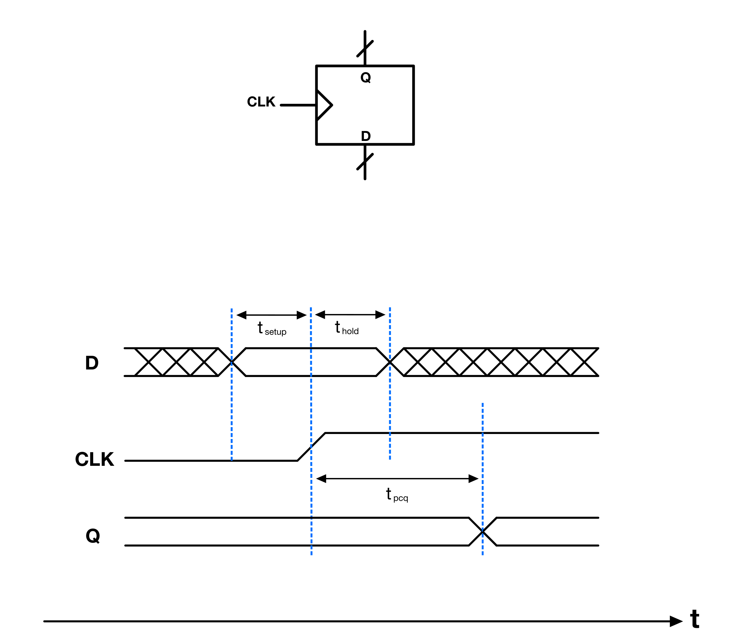
In the context of synchronous sequential circuits (like a flip-flop), the clock-to-Q propagation delay ($t_{pcq}$) refers to the time from the clock’s active edge until the output stabilizes to its new state.
A synchronous sequential circuit has a somewhat strict definition, but for this discussion, view them as systems where all registers synchronize to a common clock signal.
Setup and Hold Time
In addition to $t_{pcq}$, there are two other important timing considerations: setup time ($t_{setup}$) and hold time ($t_{hold}$):
- The setup time ($t_{setup}$) is the minimum time before the clock edge by which the input data must remain stable to be correctly captured by a circuit.
- The hold time ($t_{hold}$) is the minimum duration for which the input data must remain stable after the clock edge.
Critical Path
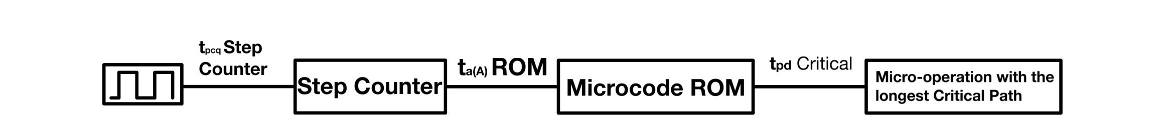
The critical path is the slowest signal path that must settle before the next clock edge. If the clock is too fast, some signals may not settle before the CPU tries to latch the next value. The critical path of my CPU contains the following:
I set out to use the timing constraints of the chips in my build’s critical path at 4.5V and 25 degrees Celsius. However, some of the datasheets for the chips I used provide switching information only for 5V.
In general, lower temperatures can reduce resistance inside a chip by giving electrons a cleaner path through the material. With fewer collisions, electron mobility improves, and signals can move faster.
Also, increasing the supply voltage, within the chip limit of course👀, usually results in increased speed as well.A higher voltage charges and discharges internal capacitances faster, which allows the transistors to switch more quickly.
The voltage on my rails is around 4.90 V, which is higher than the 4.5 V value I use for timing estimates. The CPU will also always run indoors at room temperature.
For that reason, I treat the 4.5 V / 25°C timing values as a conservative estimate where they are available. When a datasheet only gives a 5 V value, I use that value and leave some practical margin instead of trying to push the clock to the calculated limit.
The HIGH phase of the clock just latches data prepared during the LOW phase. Therefore, the critical path for the HIGH phase is the chip with the longest $t_{pcq}$ latched during this phase. The register with the highest $t_{pcq}$ is the 74HCT194 shift reg, with a $t_{pcq}$ max of 37ns.
Therefore, $t_{pcq,\text{HIGH}} = 37\text{ ns}$.
The LOW phase, on the other hand, has a critical path that depends on my instructions implementation. More specifically, it is the micro-operation across all instructions that requires the most time to complete.
The micro operations that take the most time are those that must:
- Access memory
- Output the memory content and input it to the ALU
- Input the result from the ALU to the zero detector
- Input the zero detector’s result to the flags mux
- Then write the content at the output of the flags mux to the Flags Register.
Based on the max propagation delays of the chips I’ve used, the RAM’s bus transceiver enable signal arrives $1ns$ after the RAM content reaches the transceiver’s input.
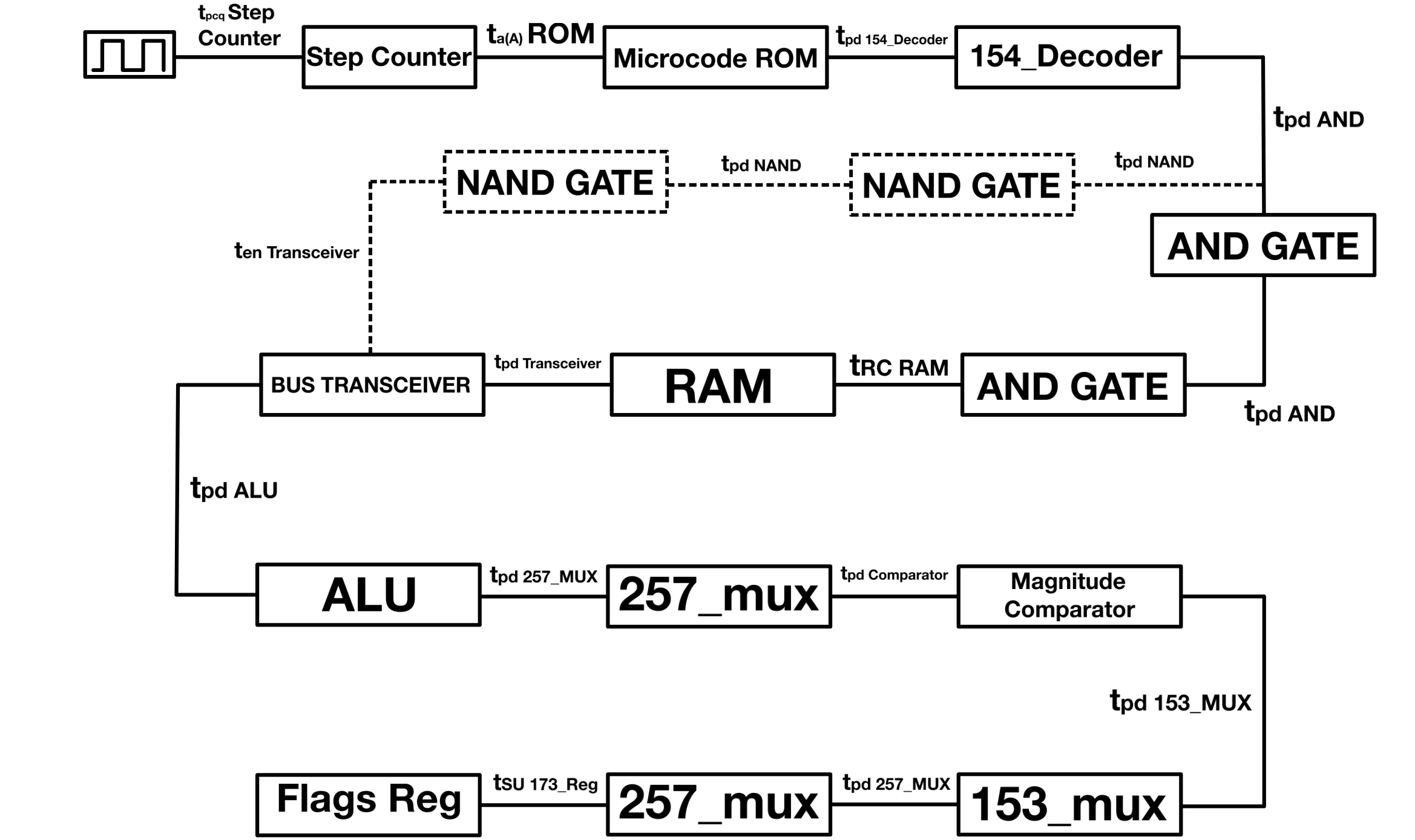
Below are the delays for the elements on the LOW-phase critical path:
74HCT161 Counter
$t_{pcq}$(4.5V): max = 39ns
TSM27C240 Control ROM
$t_{a(A)}$ Access time from address and ta(E) Access time from chip enable(5V): max = 120ns
74HCT257 4-to-16 DECODER
$t_{pHL}$ and $t_{pLH}$(4.5V): max = 35ns
74HCT08 AND
$t_{pHL}$ and $t_{pLH}$(5V): typ = 11ns; max = 18ns
UM61512A-15 RAM
$t_{RC}$ (5V) = 15ns
74HCT00 NAND
$t_{pHL}$ and $t_{pLH}$(5V): typ =18ns; max = 23ns
74HCT245 Transceiver
$t_p$(4.5V): max = 26ns
$t_{en}$(4.5V) Output enable to output: max = 32ns
74LS382 ALU
$t_{pLH}$(5V): typ = 20 ns; max = 30ns
$t_{pHL}$(5V): typ = 15 ns; max = 23ns
Using 30 ns
74HCT257 2-to-1 MUX
$t_p$(4.5V): max = 38ns
74HCT688 Comparator
$t_{pHL}$ and $t_{pLH}$(4.5V): max = 34ns;
74HCT153 MUX
$t_{pHL}$ and $t_{pLH}$ (4.5 V): max = 34 ns
74HCT173 Reg
$t_{su}$(4.5) = 18ns
    161 = 39ns
  +
    ROM = 120ns
  +
    154 = 35ns
  +
    NAND = 23ns
  +
    NAND = 23ns
  +
    ten_245 = 32ns
  +
    ALU = 30ns
  +
    257 = 38ns
  +
    ZER = 34ns
  +
    153 = 34ns
  +
    257 = 38ns
  +
    173 = 18ns
------------------
tpd LOW phase = 464ns
Therefore, $t_{pd,\text{LOW}} = 464\text{ ns}$.
$t_{pd} = t_{pcq,\text{HIGH}} + t_{pd,\text{LOW}} = 37\text{ ns} + 464\text{ ns} = 501\text{ ns}$.
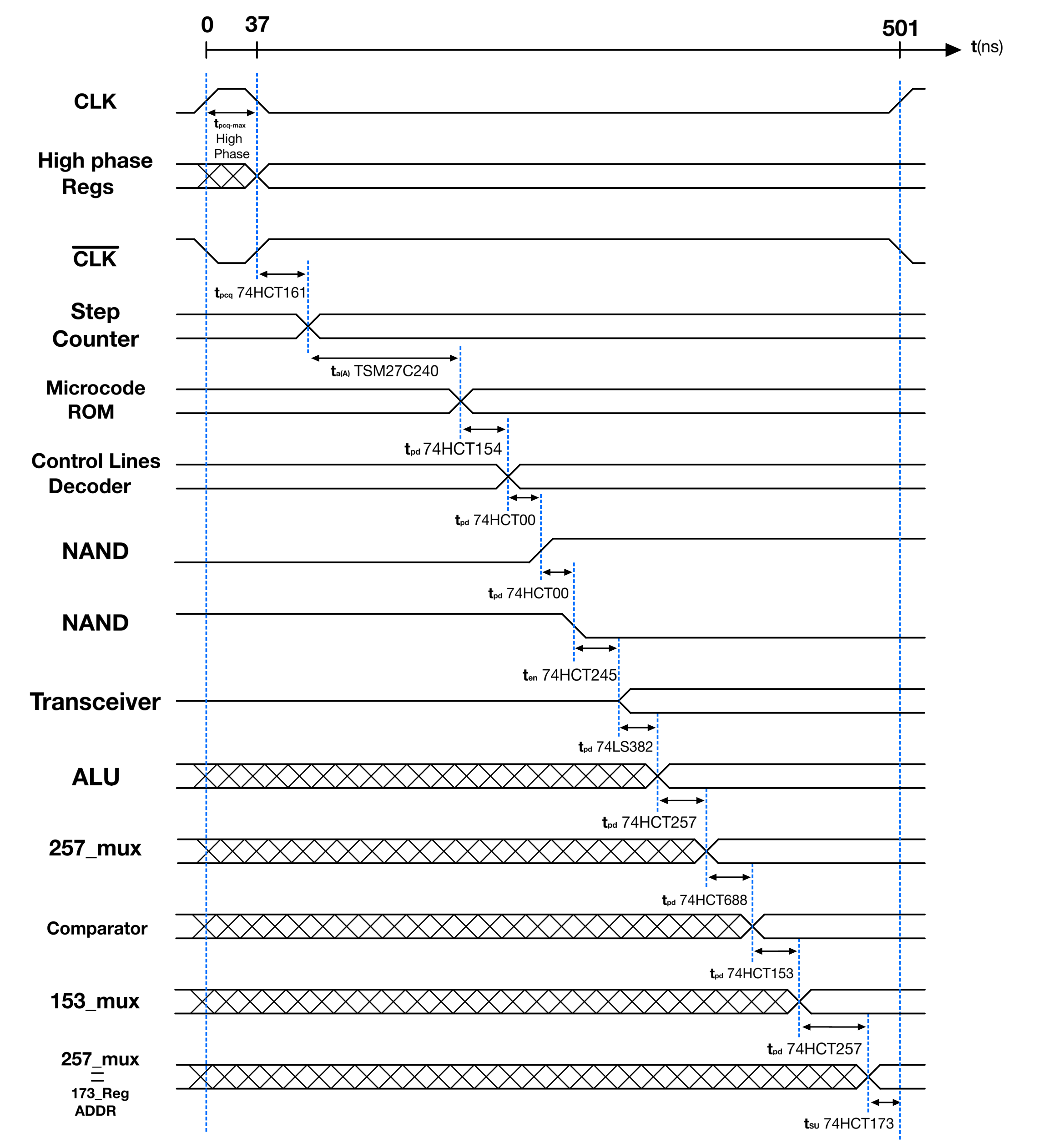
By considering only the maximum timing values, the combined propagation delay for the critical paths of both the LOW and HIGH phases amounts to 501ns. Therefore, to guarantee safe operation, the chosen clock frequency should accommodate this cumulative delay:
$f_\text{CLK} = \frac{1}{501 \times 10^{-9}\text{ s}} \approx 1.996\text{ MHz}$
The corresponding HIGH-phase duty cycle estimate is:
$100 \times \frac{37}{501} \approx 7.39\%$
Implementation
Control lines involved:
- |← HLT Halt
- |→ CLK Clock Signal
- |← ~CLW Clock speed select
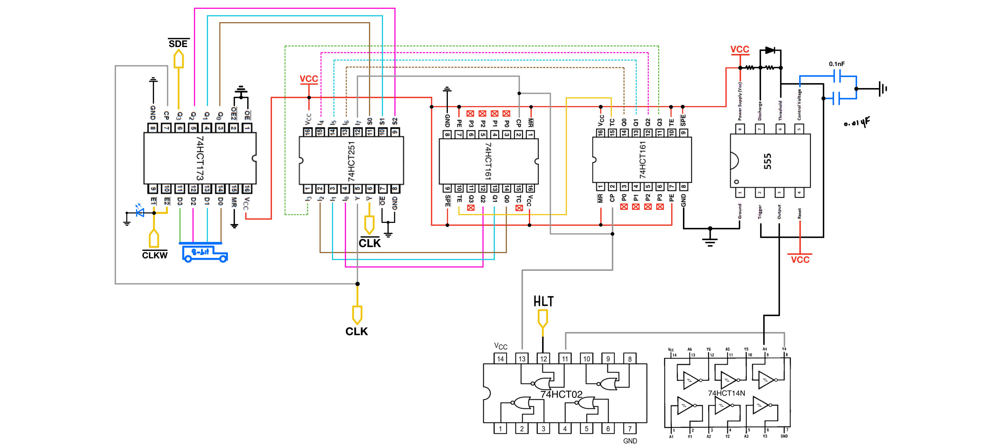
The main clock is generated by a 555 timer and then passed through an 8-bit counter made from two 4-bit counters. Each counter output divides the input clock by another factor of two. Those divided clock signals feed an 8-to-1 multiplexer, and the CPU selects one of them as the active clock rate. The multiplexer also provides an inverted output, which I use for the microstep counter clock. The mux select lines come from a 4-bit register connected to the data bus. The most significant bit of that register controls whether the segmented display is enabled (I plan to use it to switch the display output from unsigned to signed two’s complement).
Given that the counter begins by dividing the clock frequency by two, I’ve directly connected the original clock signal from the 555 timer to the MSB of the mux. The remaining seven inputs of the mux are connected from the seven most significant bits of the counter.
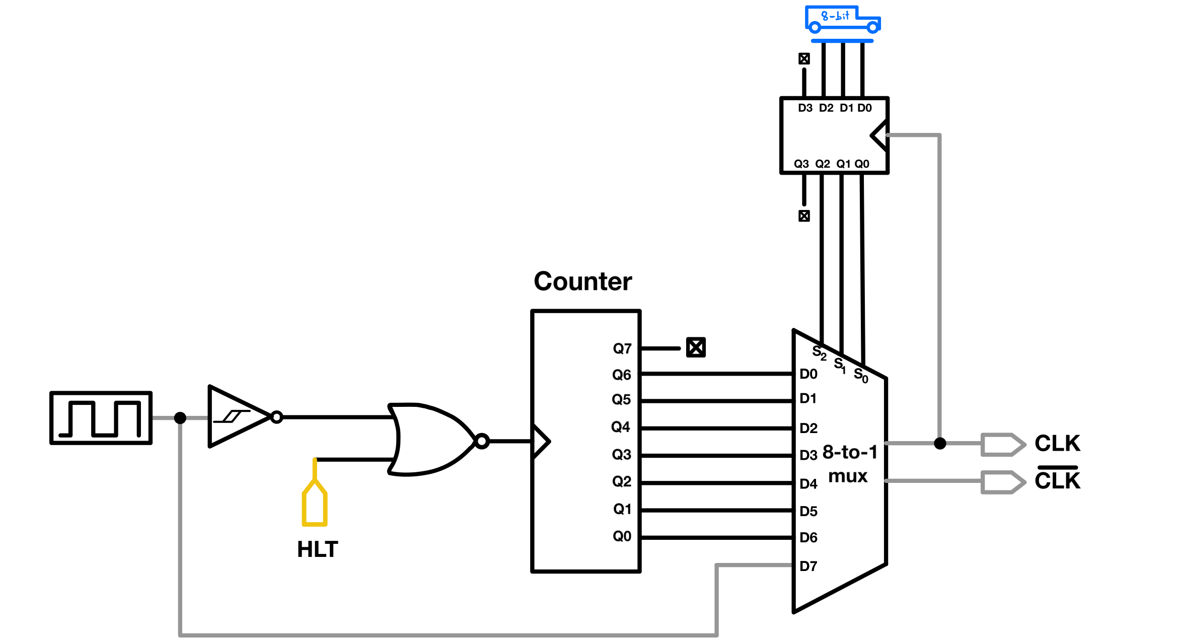
Note: I built this module with a NOR gate and an inverter to use an available NOR IC from a flip-flop on the breadboard directly beneath it. I chose a Schmitt trigger inverter simply because I lacked standard HCT04 NOT ICs. A regular NOT gate works fine here, though the Schmitt trigger helps mitigate potential noise from the 555 timer.
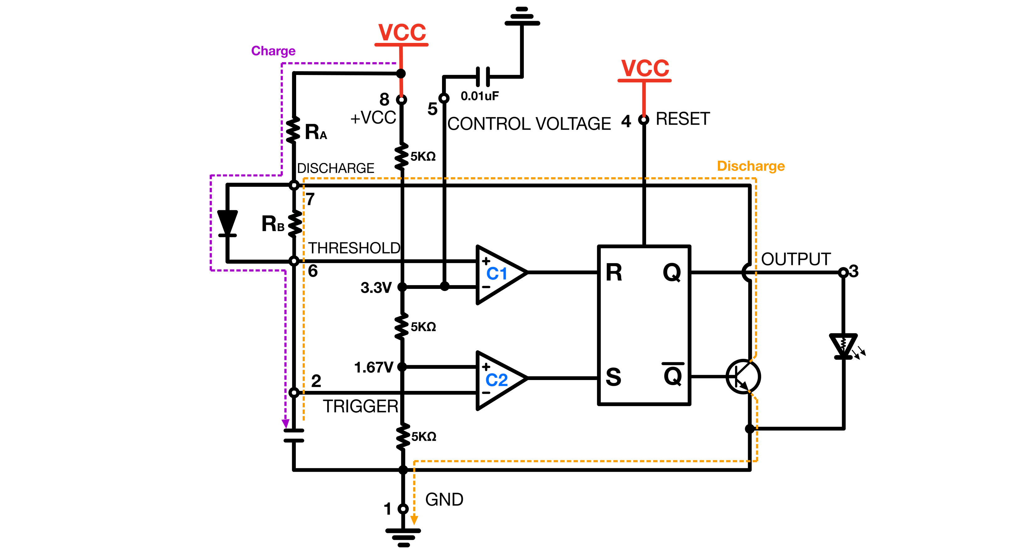
The permanent clock’s timer configuration is very similar to that of the astable debugging clock. The bypass diode forces the capacitor to charge through ${R_A}$ and discharge through $R_B$.
With the bypass diode:
$t_\text{charge} = 0.693 × R_AC$
$t_\text{discharge} = 0.693 × R_BC$
$f = 1.44/((R_A + R_B)C)$
Let $(R_A + R_B)$ be $R_t$
⇒ $1.996\text{ MHz} = 1.44/(R_tC)$
⇒ $R_t = 1.44/(C × 1.996\text{ MHZ})$
⇒ $R_t = (7.214 × 10^{-7}s)/C$
Note: Because capacitance and resistance are inversely proportional, multiplying any given capacitance $C$ by a factor of $n$ ($nC$) means the total resistance can divide by that same factor $n$.
For a 0.1nF capacitor:
⇒ $R_t = (0.72144 μs/0.1nF)$
⇒ $R_t = 7.214 KΩ$
Since the duty cycle is 7.385%, the charging and discharging resistances must be:
$R_\text{charge}$ = $7.214 \text{ KΩ} × 7.385/100 = 0.533\text{ KΩ}$
$R_\text{discharge}$ = $R_t - R_\text{charge} = 7.214\text{ KΩ} - 0.533\text{ KΩ} = 6.682\text{ KΩ}$
Overclocking
The $1.996 \text{ MHz}$ estimate above is the calculated clock rate based on the conservative/pessimistic critical-path timing model.
The 555 timer that I use has a maximum frequency of $3\text{ MHz}$. So I tried out higher clock rates to see up to what point the CPU could still hold up.
The closer the 555 gets to its maximum frequency, the less accurate its formulas become. I tried many combinations of $R_A$, $R_B$, and capacitors to target a 2.5 MHz clock rate. The lower the value of any single component (the capacitor or a resistor), the more unpredictable the clock rate became. Ultimately, the choice of diode mattered more than anything else.
After many trial and error attempts, I ended up with the following values:
$C = 47\text{ pF}$
$R_A = 47\text{ Ω}$ using a 2 W resistor to avoid overheating from the large current flow.
$R_B = 2.481\text{ kΩ}$ using $3.3\text{ kΩ}$ and $10\text{ kΩ}$ in parallel.
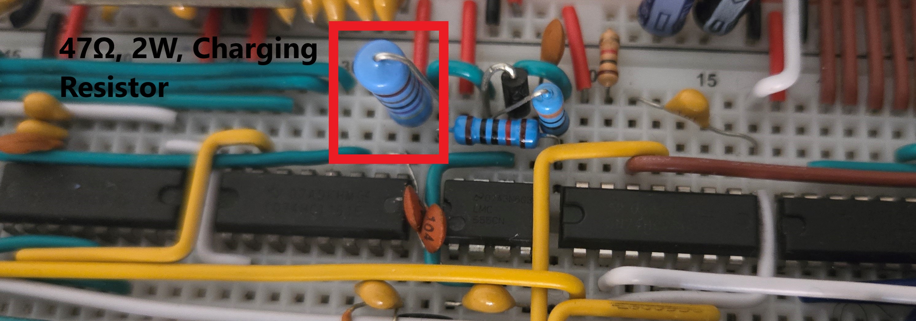
With the values above and an ideal diode, the clock rate should exceed 10MHz (which is impossible for the 555). However, I observed the following in practice:
$f = 2.2\text{ MHz}$
$\text{Duty cycle} = 22\%$
I verified that the LOW phase can be as short as $346\text{ ns}$. Since the HIGH phase only needs about $37\text{ ns}$ in my timing model, a stable overclock requires at least a $37\text{ ns}$ HIGH phase and a $346\text{ ns}$ LOW phase. The practical timing limit is therefore about $\frac{1}{37\text{ ns} + 346\text{ ns}} \approx 2.6\text{ MHz}$.
ICs
1x LMC555CN CMOS Single 555 Timer Low Power DIP-8 (Jameco, Datasheet)
1x 74HCT251 High-Speed CMOS Logic 8-Input Multiplexer (Digikey, Datasheet)
2x 74HCT161, Synchronous 4-Bit Binary Counter, (Digikey, Datasheet)
1x 74HCT173, 4-Bit D-type Registers with tri-state Outputs, (Digikey, Datasheet)
1x 74HCT14 Hex Schmitt-Trigger Inverters (Digikey, Datasheet)(Shared with Control Logic)
1x 74HCT02 Quadruple 2-Input Positive-NOR Gates (Digikey, Datasheet) (Shared with Control Logic)