Bus & General Purpose Registers
Basics Primer
As mentioned in the overview, my F8-BB build has an 8-bit data bus and a 16-bit system/memory bus. The name “data bus” is somewhat loose, since all computer buses carry data of some kind. In this build, I use “data bus” to refer to the 8-bit bus that carries register values, instruction operands, memory data, and I/O data. The 16-bit system/memory bus carries addresses and connects the CPU to memory-related modules.
The 16-bit address bus, explained in more detail in the RAM post, is an enhancement to the memory capacity without making the design overly complex. In simple terms, a 16-bit address bus allows the CPU to access a larger memory space compared to an 8-bit address bus. With 16 bits, the CPU can address up to 65,536 ($2^{16}$) individual memory locations, which provides ample space to store and retrieve data and instructions.
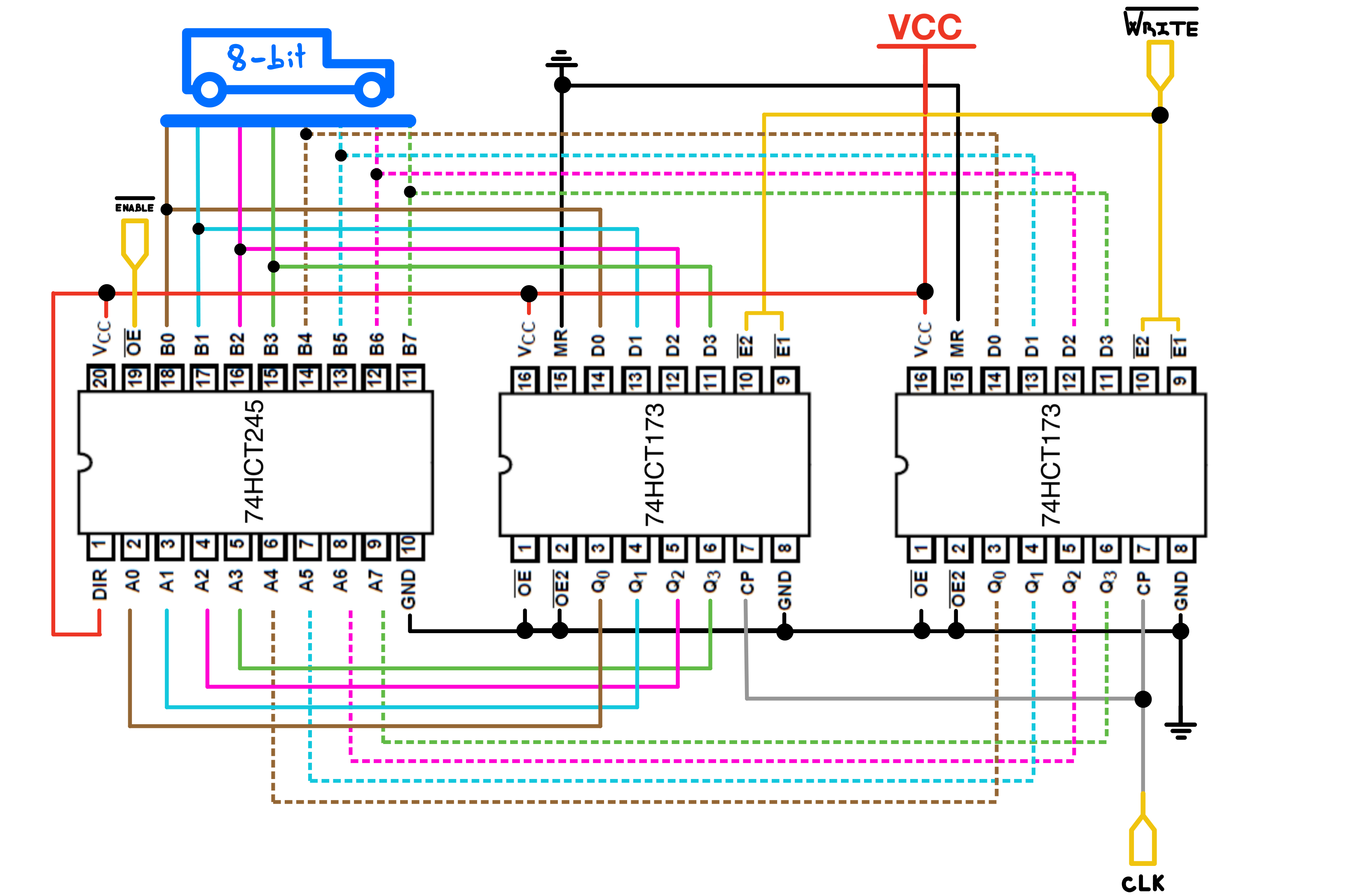
F8-BB contains five general-purpose registers (GPRs): A, B, C, D, and E, though register E supports only a limited set of instructions. All GPRs can read from and write to the 8-bit data bus. Four of them are dual 74HCT173(173) which I had assembled when initially building the SAP-1, and the last one is a 74HCT574(574).
Implementation
The 173 is a 4-bit register, so two chips share common control pins to make a single 8-bit register. Although the 173s have tri-state outputs, their outputs remain active so the register contents can appear on LEDs. A 74HCT245 transceiver sits between the 173s and the bus and makes the final output enable, which prevents the LEDs and register outputs from interfering with bus activity.
| Pin No | Pin Name | Description |
|---|---|---|
| 1 | DIR | Direction select(A to B, or B to A) |
| 2, 3, 4, 5, 6,7,8,9 | A1, A2, A3, A4, A5, A6, A7, A8 | Input/Output Pin 1, 2, 3, 4, 5, 6, 7, 8 |
| 10 | GND | Ground Pin |
| 11, 12, 13, 14, 15, 16, 17, 18 | B1, B2, B3, B4, B5, B6, B7, B8 | Output/Input Pin 1, 2, 3, 4, 5, 6, 7, 8 |
| 19 | ~E | Active Low Input Enable Pin |
| 20 | VCC | Chip Supply Voltage |
Table 1: 74HCT245 Octal Bus Transceivers, Pin Configuration
| Pin No | Pin Name | Description |
|---|---|---|
| 1, 2 | ~OE, ~OE2 | Active Low Output Enable Input 1 and 2 |
| 3, 4, 5, 6 | Q0, Q1, Q2, Q3 | Output Pin 0, 1, 2, 3 |
| 7 | CP | Clock Pulse Input |
| 8 | GND | Ground Pin |
| 9 | ~E1, ~E2 | Active Low Input Enable Pin 1, 2 |
| 11, 12, 13, 14 | D3, D4, D5, D6 | Data Input 3, 2, 1, 0 |
| 15 | MR | Master Reset Input |
| 16 | VCC | Chip Supply Voltage |
Table 2: 74HCT173 Pin Configuration
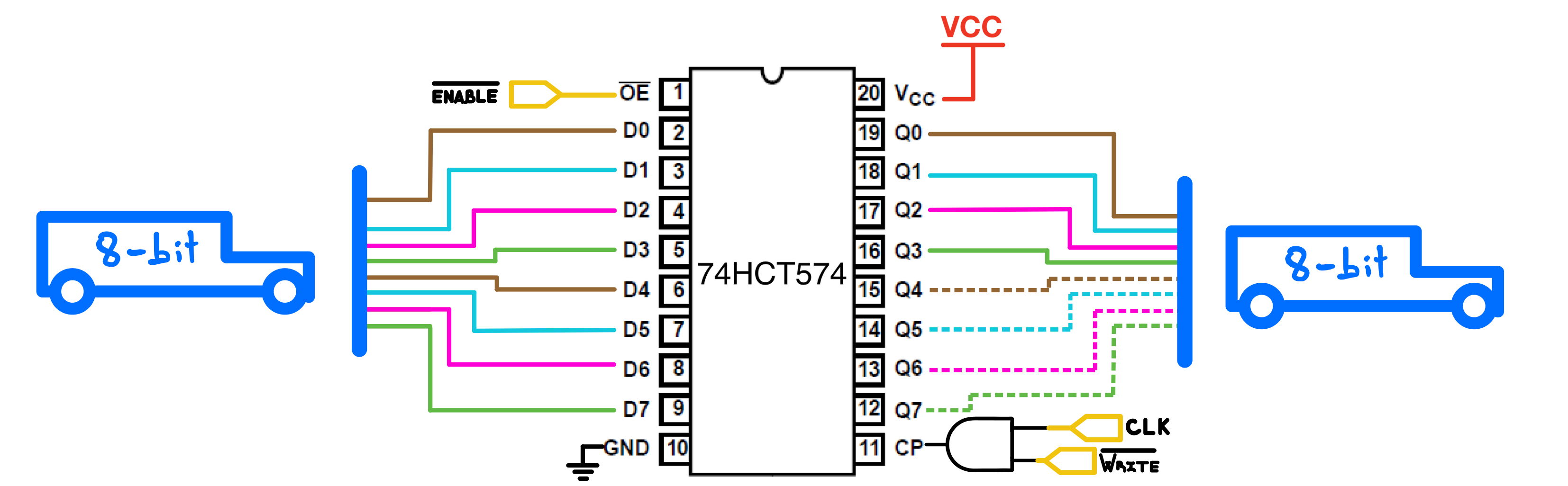
Unlike the 74HCT173, the 74HCT574 does not have a data-enable input. Its output-enable pin controls whether the stored value appears at the outputs, but it does not prevent the register from loading new data on a rising clock edge. By default, the clock pin CP acts as both an enable and a clock input. This means at every rising clock edge, whatever appears on the data pins overwrites the register’s content. To avoid this, I AND the clock with the “write” control line for each 574, so the register only loads during a write operation.
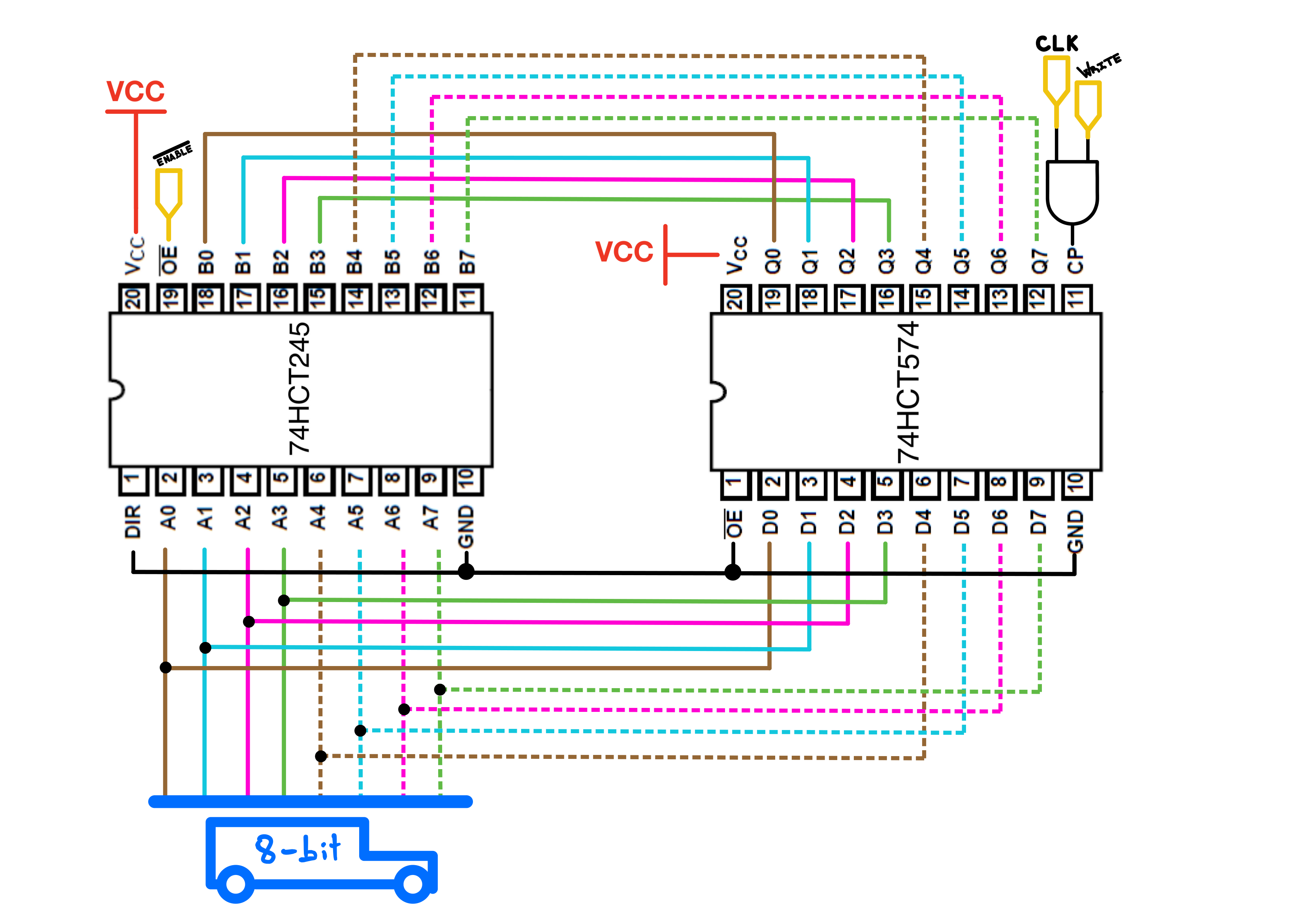
Unlike some other 8-bit register ICs with built-in gated enables, the 74HCT574 has a very clean pin layout: All inputs and outputs are aligned on opposite sides of the IC, which makes it very breadboard-friendly, just like the 74HCT173. Some of the 574s in the F8-BB are used without a transceiver due to space constraints on the breadboards.
| Pin No | Pin Name | Description |
|---|---|---|
| 1 | ~OE | Active Low Tri State Output Enable Pin |
| 2, 3, 4, 5, 6,7,8,9 | D0, D1, D2, D3, D4, D5, D6, D7 | Data Input Pin 1, 2, 3, 4, 5, 6, 7, 8 |
| 10 | GND | Ground Pin |
| 11 | CP | Clock Pulse Input |
| 12, 13, 14, 15, 16, 17, 18, 19 | O0, O1, O2, O3, O4, O5, O6, O7 | Tristate Output Pin 0, 1, 2, 3, 4, 5, 6, 7 |
| 20 | VCC | Chip Supply Voltage |
Table 3: 74HCT574 8-bit Octal D-Type Flip-Flop Pin Configuration
ICs
8x 74HCT173, 4-Bit D-type Registers with tri-state Outputs, (Digikey, Datasheet)
1x 74HCT574, 8-bit Octal D-Type Flip-Flop, 3-State (Digikey, Datasheet)
4x 74HCT245, Octal Bus Transceivers With 3-State Outputs, (Digikey, Datasheet)