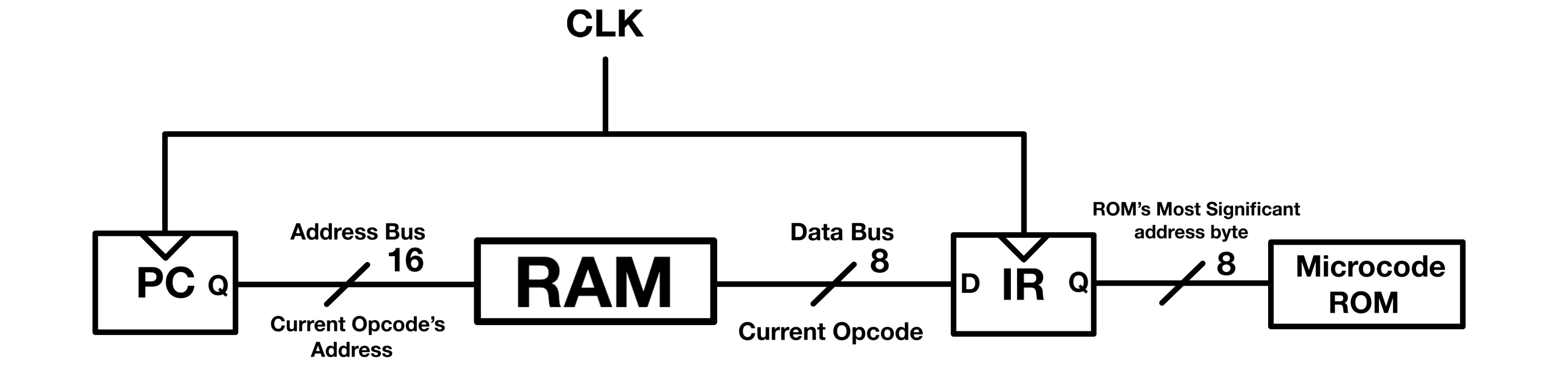
Control Unit & Instruction Register
Basics Primer
The Control Unit (CU) is what ties the CPU modules together. It does not store program data or perform arithmetic itself. Instead, it reads the current instruction and produces the control signals that tell the other modules what to do. Among other things, these signals decide which registers place data on the bus, which registers latch new values, whether memory is read or written, what operation the ALU performs, and how the Program Counter or Stack Pointer changes.
The exact design of a Control Unit varies from one CPU to another. Some CPUs use hardwired control logic, while others use microcode.
In a hardwired control unit, the instruction logic is built directly from gates and other fixed logic circuits. That approach can be fast, but changes to the instruction set often require hardware changes. In a microcoded control unit, each instruction maps to a short sequence of stored control words called microcode. Each control word activates the signals required for one step of the instruction. A microcoded design is often easier to design and modify.
The Instruction Register (IR) stores the instruction byte currently under control-unit decode. After the CPU fetches an opcode from memory, that opcode is loaded into the IR. The Control Unit then uses the value in the IR to select the correct microcode sequence for that instruction. The opcode defines the operation to perform, such as loading a register, writing to memory, jumping to another address, or performing an ALU operation.
Some instructions consist only of an opcode, while others require extra bytes after the opcode. Those extra bytes may represent an immediate value, a memory address, or other information needed by the instruction. The IR usually holds the opcode, while the CPU fetches any additional operand bytes during later steps of the instruction.
The Von Neumann architecture is a foundational computer architecture model that dates back to the mid-1940s. Its central idea is that program instructions and data share the same memory space. Most general-purpose computers still use a Von Neumann-style stored-program model, at least from the programmer’s point of view, even when the internal hardware includes separate instruction and data caches for performance.
A common comparison is the Harvard architecture, which uses separate memory spaces for instructions and data.
My CPU, being based on the SAPs is an example of a computer that follows the Von Neumann architecture.
The Von Neumann Fetch-and-Execute Cycle
Here’s a simplified outline of the steps in the Fetch-and-Execute cycle in a basic Von Neumann architecture:
Note: The term “fetch-and-execute cycle” describes the full process the CPU uses to run an instruction. In this context, “cycle” does not mean a single clock cycle. One fetch-and-execute cycle may require several clock cycles because the CPU must fetch the instruction, decode it, and perform the required operation.
1- Fetch
The CPU first copies the address held in the Program Counter (PC) into the Memory Address Register (MAR). Then, memory at that address is read into the Instruction Register (IR). After that, the PC increments to the next memory address. For single-byte instructions, that address is usually the next instruction. For multi-byte instructions, it may instead point to an operand byte that belongs to the current instruction.
2- Decode
The Control Unit decodes the opcode stored in the IR to determine which operation the CPU should perform. Depending on the instruction format, the CPU may also fetch additional operand bytes after the opcode, such as an immediate value or a memory address. It’s important to note that the decoding process varies depending on the complexity and design of the CU and the instruction set architecture of the CPU.
3- Execute
To now execute the fetched and decoded instruction, the CU issues control signals to relevant parts of the CPU to carry out the instruction. The signals carry out the required steps, such as directing the Arithmetic Logic Unit (ALU) to perform a computation or moving data between registers. The execution process is closely tied to the specifics of the instruction set and the architecture of the CPU.
The Instruction register
My instruction register is extremely simple. As mentioned in the primer, it holds the instruction currently being executed. On my build, the IR’s output is permanently tied only to the microcode ROM. That point requires a small clarification about what an instruction is.
Difference Between an Opcode and an Instruction
An instruction is simply a complete command that tells the CPU what to do. It consists of an opcode and, often, additional information like operand addresses or immediate values. The opcode, or operation code, is part of the instruction that specifies the operation to be performed.
For example, consider an instruction like ADD A, B. Here, ADD is the opcode that tells the CPU to perform an addition operation, while A and B are operands that specify where the data for the operation comes from or goes to.
In binary form(Machine code), the instruction might look something like 0b00011011, where a part of the binary code (e.g., 0b0001) represents the opcode for ADD, and the rest (0b1011) indicates the operands A and B.
Not all instructions require operands. Some instructions, like NOP (no operation) or HLT (halt), consist only of an opcode. For example, NOP might be represented as 0b0010 in binary form, with no additional operand information needed.
Instructions Encoding On My CPU
In my design I do not structurally split the instruction into an opcode and operand. Instead, each instruction byte is treated as a unique opcode that selects the corresponding microcode sequence.
Operand handling happens through additional memory reads. If an instruction needs an immediate value or a memory address, the CPU increments the PC and fetches the required operand byte or bytes from memory after the opcode. In other words, the operand is not packed into the same instruction byte; it follows the opcode in memory.
To understand my encoding, let’s compare Ben Eater’s SAP-1 LDA instruction with the equivalent instruction in my CPU. LDA means “load register A” with data from a memory address.
A later post on assembly explains how mnemonics such as ADD and LDA become numeric machine-code values. For now, it is enough to know that these mnemonics are written in assembly language, and an assembler translates them into the binary values the CPU can execute.
SAP-1’s LDA
As a reminder, the SAP-1 is an 8-bit CPU with 16 bytes of RAM. Because it only needs to address 16 memory locations, it uses a 4-bit Program Counter and a 4-bit Memory Address Register.
The SAP-1 instruction register is 8 bits wide, but the instruction format is split into two 4-bit fields. The upper four bits form the opcode, and the lower four bits form the operand. In Ben Eater’S SAP-1 implementation, the opcode for LDA is 0b0001 .
For example, an LDA instruction that loads register A from memory address 0b1010 would be encoded as 0b00011010. The upper nibble, 0b0001, selects the LDA operation. The lower nibble, 0b1010, supplies the memory address.
During execution, the opcode selects the microcode sequence for the load operation. The operand is then loaded into the Memory Address Register, so the RAM location at address 0b1010 can place its data on the bus and load register A.
My LDA Equivalent
In my CPU, the equivalent instruction is MOV $A, [address]. I compare it to SAP-1’s LDA because both instructions load register A from memory.
Instead of splitting one instruction byte into an opcode field and an operand field, my design gives each instruction form its own full 8-bit opcode. The operand is not packed into the same instruction byte. It follows the opcode in memory.
For MOV $A, [address], the CPU first fetches the opcode. It then fetches the next two bytes from memory as the 16-bit address operand: lower byte first, upper byte second. Those two bytes are loaded into the Bridge Register. After that, the Bridge Register drives the memory/system bus, and the value stored at that memory address is loaded into register A.
For example, to load $A from memory address 0x0008, memory would contain the opcode for MOV $A, [address], followed by 0x08 and 0x00.
The Microcode ROM
The Microcode ROM provides a low-level control mechanism that defines how the CPU behaves during instruction execution. It contains a set of predefined values that appear on the ROM’s output pins as control signals for each step of every instruction.
In this CPU, the Microcode ROM address is formed from four groups of signals:
- The content of the Instruction Register(8 bits)
- The content of the Flags Register(4 bits)
- The Interrupt Inhibit and Interrupt Request Flags(2 bits)
- The content of the Microcode Step Counter(4 bits)
Since the ROM has 18 address inputs, it contains $2^18$, or $262,144$, addressable entries. Each entry has a defined output value, even if some instruction, flag, interrupt, or step combinations are not used during normal execution.
Flags
Flags are status bits that record conditions produced by CPU operations. For example, a flag may show whether an ALU result was zero, negative, produced a carry, or caused an overflow. The Microcode ROM uses these flag values as part of its address input, so the same instruction can select different control words depending on the current CPU state.
This is especially important for conditional instructions. A conditional jump, for example, can follow one microcode path when a flag is set and another path when that flag is clear. In that way, the flags help the Control Unit choose the correct sequence of control signals for the current instruction and CPU state.
Types of Flags on my CPU
ALU Flags
ALU flags record the result of arithmetic and logic operations. They are especially useful for conditional instructions, where the next action depends on the result of a previous operation. These flags are described in more detail in the “ALU & Flags” post.
- Zero Flag (Z): Set when the result of an operation is zero.
- Overflow Flag (O): Set when a signed arithmetic result cannot be represented in the available number of bits.
- Negative(Sign) Flag (N): Set according to the most significant bit of the result. In two’s-complement arithmetic, this bit represents the sign of the value.
- Carry Flag (C): Set according to the carry behavior of the ALU. For addition, it indicates a carry out of the most significant bit. For subtraction on this CPU, it behaves as a no-borrow flag.
Interrupt-Related Flags:
More information about the interrupt flags and interrupt mechanism will be made available in a future I/O post.
- II (Interrupt Inhibit): Indicates whether interrupts are currently inhibited.
- IRQ (Interrupt Request): Signals whether an interrupt request has been made.
Micro Steps
Micro-steps, also called micro-operations, are the smaller control stages that make up the execution of a single instruction. Each micro-step corresponds to one control word from the Microcode ROM. That control word activates the control lines needed for that stage of the instruction.
In my CPU, a new micro-step begins on the falling edge of the clock. After the micro-step counter changes, the new address selects the next control word in the Microcode ROM. The control signals then settle during the low phase of the clock, before data is latched on the next rising edge.
The Micro-Step Counter
The micro-step counter tracks the current stage of an instruction. It lets the CPU step through the correct sequence of control words for the instruction currently held in the Instruction Register.
On the falling edge of the clock, the micro-step counter increments. The new counter value becomes part of the address into the Microcode ROM, so the ROM outputs the control word for the next micro-step. During the low phase of the clock, those control signals select the required bus sources, register inputs, memory controls, ALU operation, or other CPU actions. On the next rising edge, the selected registers latch their new values.
Clock Behavior:
- On the Falling Edge of the Clock: The micro-step counter increments, which selects the next control word in the Microcode ROM.
- On the Low Phase of the Clock: The selected control signals remain active and settle before the next rising edge.
- On the Rising Edge of the Clock: Registers and other clocked parts of the CPU latch data according to the active control signals.
For clarity, the next section looks at the micro-steps used by SAP-1’s LDA instruction.
Note: In simple Von Neumann-style CPUs such as the SAP-1, the fetch phase is usually the same for every instruction. The CPU reads the next instruction from memory, places it into the Instruction Register, and then uses the opcode to select the correct execution sequence. After that point, the micro-steps depend on the instruction.
The Fetch-And-Execute Cycle On The SAP-1
Base Assumption
- The Program Counter is initially at address
0b0000. - Every instruction begins with the same fetch phase. As long as the micro-step counter is at step 0 or step 1, the Microcode ROM outputs the fetch control lines, regardless of the opcode currently held in the Instruction Register.
The program and data are stored in RAM as follows:
RAM Address Content 0b0000 0b00011000 0b0001 xxxx 0b0010 xxxx 0b0011 xxxx 0b0100 xxxx 0b0101 xxxx 0b0110 xxxx 0b0111 xxxx 0b1000 0b11011000
xxxx = Don’t care.
The instruction at address 0b0000 is 0b00011000. The upper nibble, 0b0001, is the opcode for LDA. The lower nibble, 0b1000, is the operand, which points to RAM address 0b1000.
Below are the control lines involved in the LDA instruction:
- MI (MAR In): Loads the Memory address register on the next clock edge.
- CO (Program Counter Out): Outputs the content of the Program Counter to the bus.
- RO (RAM Out): Outputs the content of the RAM at the specified address to the bus.
- II (Instruction Register In): Loads the Instruction Register on the next clock edge with the content at its input.
- CE (Counter Enable): Increments the Program Counter by one on the next clock edge.
- IO (Instruction Register Out): Outputs the content of the Instruction Register to the bus.
- AI (A Register In): Loads data into the A register.
For this example, the CPU executes LDA 0b1000, which loads register A with the value stored at RAM address 0b1000.
1. Fetch
At micro-step 0: PC = 0b0000, MAR = xxxx
From the falling edge of the clock to the end of the LOW phase:
The Microcode ROM asserts CO and MI. The Program Counter places 0b0000 on the bus, and that value reaches the input of the Memory Address Register.
On the next rising edge:
The MAR latches 0b0000.
At micro-step 1: PC = 0b0000, MAR = 0b0000
From the falling edge of the clock to the end of the LOW phase:
The Microcode ROM asserts RO, II, and CE. RAM places the content at address 0b0000 on the bus. That value is 0b00011000, the encoded LDA 0b1000 instruction.
On the next rising edge:
The Instruction Register latches 0b00011000, and the Program Counter increments to 0b0001.
At the end of the fetch phase, the IR contains the instruction byte. The upper nibble, 0b0001, selects the LDA microcode sequence. The lower nibble, 0b1000, remains available as the memory address operand.
2. Execute
At micro-step 2: PC = 0b0001, MAR = 0b0000, IR = 0b00011000
From the falling edge of the clock to the end of the LOW phase:
The Microcode ROM now selects step 2 of the LDA sequence because the opcode field is 0b0001. It asserts IO and MI. The Instruction Register places its lower nibble, 0b1000, on the bus, and that value reaches the input of the MAR.
On the next rising edge:
The MAR latches 0b1000.
At micro-step 3: PC = 0b0001, MAR = 0b1000, IR = 0b00011000
From the falling edge of the clock to the end of the LOW phase:
The Microcode ROM selects step 3 of the LDA sequence. It asserts RO and AI. RAM places the content at address 0b1000 on the bus. In this example, that value is 0b11011000.
On the next rising edge:
Register A latches 0b11011000. The LDA instruction is now complete.
If the program should stop immediately after this instruction, a HLT instruction should be placed at RAM address 0b0001, because the Program Counter already points there after the fetch phase.
The Fetch-And-Execute Cycle On My CPU
As mentioned in the RAM & Bridge Register, my build does not use a MAR, because it has a dedicated memory/system bus. This means that, the content of the Program Counter can be directly presented to the RAM’s input pins without any intermediary steps.
In other words, the instruction fetching is done in one cycle.
The execute phase follows the same general idea as the SAP-1 example: each micro-step activates a specific set of control lines. The exact control lines differ because my CPU has a different ISA, a 16-bit address space, and a Bridge Register used to place full addresses on the memory/system bus.
For this example, let’s look at my CPU’s equivalent of LDA: MOV $A, [address]. The instruction loads register A with the byte stored at a 16-bit memory address.
Base Assumption
The program is stored in RAM as follows:
| RAM Address | Content | Meaning |
|---|---|---|
0b0000000000000000 or 0x0000 | 0b10100101 or 0xA5 | Opcode for MOV $A, [address] |
0b0000000000000001 or 0x0001 | 0b00001000 or 0x08 | Lower byte of address operand |
0b0000000000000010 or 0x0002 | 0b00000000 or 0x00 | Upper byte of address operand |
0b0000000000000011 or 0x0003 | xxxxxxxx | Don’t care / next instruction |
0b0000000000000100 or 0x0004 | xxxxxxxx | Don’t care |
0b0000000000000101 or 0x0005 | xxxxxxxx | Don’t care |
0b0000000000000110 or 0x0006 | xxxxxxxx | Don’t care |
0b0000000000000111 or 0x0007 | xxxxxxxx | Don’t care |
0b0000000000001000 or 0x0008 | 0b11011000 or 0xD8 | Data loaded into register A |
xxxxxxxx = Don’t care.
All other assumptions are similar to those made in the SAP-1 example.
Below are the control lines involved in MOV $A, [address]:
- PCE (Program Counter Enable): Places the Program Counter’s content on the memory/system bus.
- PCC (Program Counter Count Up): Increments the Program Counter by 1.
- ME (Memory Enable): Places the selected memory byte on the data bus.
- BRlW (Bridge Lower Write): Loads the byte on the data bus into the lower byte of the Bridge Register.
- BRhW (Bridge Upper Write): Loads the byte on the data bus into the upper byte of the Bridge Register.
- BRE (Bridge Enable): Places the Bridge Register’s 16-bit content on the memory/system bus.
- AW (A Register Write): Loads the byte on the data bus into register A.
- IR_in (Instruction Register In): Loads the byte on the data bus into the Instruction Register.
- ScR (Step Counter Reset): Resets the micro-step counter.
For this example, the CPU executes MOV $A, [0x0008], which loads register A with the byte stored at memory address 0x0008.
1. Fetch
At micro-step 0: PC = 0x0000
From the falling edge of the clock to the end of the LOW phase:
The Microcode ROM asserts PCE, ME, IR_in, and PCC. The Program Counter places 0x0000 on the memory/system bus, so RAM address 0x0000 is selected. RAM then places the byte at that address, 0xA5, on the data bus.
On the next rising edge:
The Instruction Register latches 0xA5, which is the opcode for MOV $A, [address]. The Program Counter increments to 0x0001.
2. Execute
At micro-step 1: PC = 0x0001
From the falling edge of the clock to the end of the LOW phase:
The Microcode ROM asserts PCE, ME, BRlW, and PCC. The Program Counter places 0x0001 on the memory/system bus, so RAM address 0x0001 is selected. RAM then places 0x08, the lower byte of the address operand, on the data bus.
On the next rising edge:
The lower byte of the Bridge Register latches 0x08. The Program Counter increments to 0x0002.
At micro-step 2: PC = 0x0002
From the falling edge of the clock to the end of the LOW phase:
The Microcode ROM asserts PCE, ME, and BRhW. The Program Counter places 0x0002 on the memory/system bus, so RAM address 0x0002 is selected. RAM then places 0x00, the upper byte of the address operand, on the data bus.
On the next rising edge:
The upper byte of the Bridge Register latches 0x00. The Bridge Register now contains the full 16-bit address 0x0008. The Program Counter remains at 0x0002 during this step.
At micro-step 3: PC = 0x0002, BR = 0x0008
From the falling edge of the clock to the end of the LOW phase:
The Microcode ROM asserts BRE, ME, AW, and PCC. The Bridge Register places 0x0008 on the memory/system bus, so RAM address 0x0008 is selected. RAM then places the byte at that address, 0xD8, on the data bus.
On the next rising edge:
Register A latches 0xD8. The Program Counter increments to 0x0003, which is the address of the next instruction.
At micro-step 4: PC = 0x0003
From the falling edge of the clock to the end of the LOW phase:
The Microcode ROM asserts ScR, which resets the micro-step counter. The current instruction is complete, and the next fetch starts from address 0x0003.
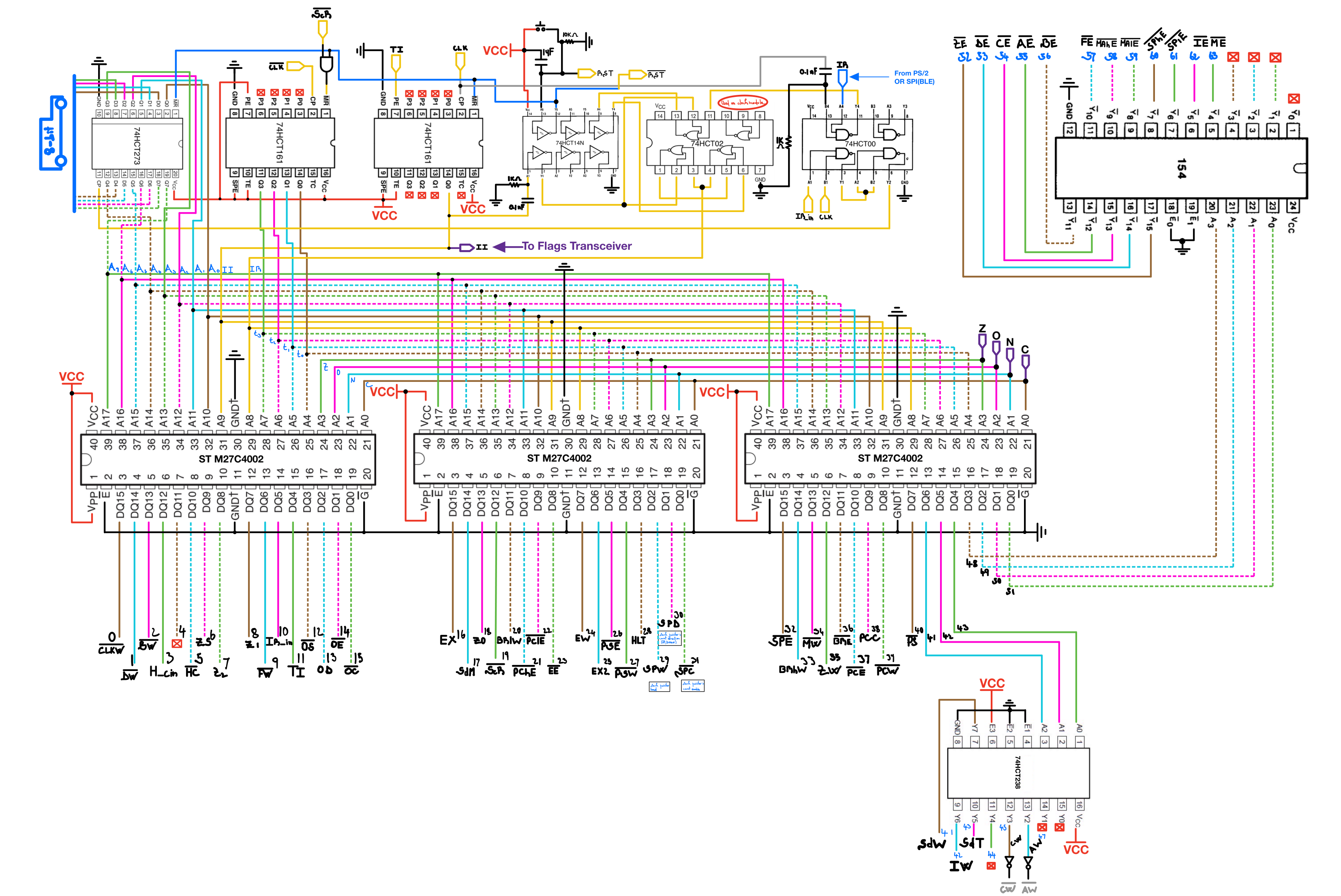
Implementation
Control signals grouped by ROM
ROM 0
| Control Signal | Description |
|---|---|
| _CLKW | Clock speed select |
| _DW | D Register (General purpose register 4) Write |
| _BW | B Register (General purpose register 2) Write |
| H_cin | Shift register carry in |
| _HC | Shift register clear/reset |
| ZS | ALU select (0: 382 ALU; 1: 194-shift register) |
| Z2 | ALU control_2 |
| Z1 | ALU control_1 |
| _FW | Flag register write/in |
| IR_in | Instruction register in |
| TI | Toggle interrupt (Sets interrupt to its opposite state) |
| _OS | OLED select (D/C# Data by default, command when asserted) |
| OR | OLED data (Read/_Write Write by default, read when asserted) |
| OE | OLED enable |
| _OC | OLED clear |
ROM 1
| Control Signal | Description |
|---|---|
| EX | Extra (Extra/Unused control line) |
| SdM | Segmented display mode (Signed/_Unsigned) |
| Z0 | ALU control_0 |
| _ScR | Step counter reset to 0 |
| BRlW | Bridge Register lower byte write |
| _PChE | Program counter upper byte enable |
| _PClE | Program counter lower byte enable |
| _EE | E Register enable |
| EW | E Register write |
| Ex2 | Extra line 2 |
| _PSE | Port selector enable |
| _PSW | Port selector write |
| HLT | Clock halt/stop |
| SPW | Stack pointer load |
| SPD | Stack pointer count direction (_up/down) |
| _SPC | Stack pointer count enable |
ROM 2
| Control Signal | Description |
|---|---|
| _SPE | Stack pointer word (16-bits) enable |
| BRhW | Bridge Register upper byte write |
| _MW | Memory write |
| ZW | Accumulator write |
| _BRE | Bridge Register word (16-bits) enable |
| _PCE | Program counter word (16-bits) enable |
| PCC | Program counter count up |
| _PCW | Program counter write/in (Jump) |
| _PS | Port select in |
| WR_2 | Write decoder A2 (74HCT238) |
| WR_1 | Write decoder A1 (74HCT238) |
| WR_0 | Write decoder A0 (74HCT238) |
| RD_3 | Read decoder A3 (74HCT154) |
| RD_2 | Read decoder A2 (74HCT154) |
| RD_1 | Read decoder A1 (74HCT154) |
| RD_0 | Read decoder A0 (74HCT154) |
Micro-Code ROM
The microcode ROM consists of three ST M27C4002 EPROMs, which I collectively refer to as the microcode ROM. Each EPROM has a 16-bit output, so the three ROMs provide 48 raw output bits.
Some of those output bits drive control lines directly. Others feed decoder chips that generate groups of mutually exclusive control signals. Since only one component should drive the data bus at a time, most data-bus enable lines are generated through a 4-to-16 decoder. That lets four ROM output bits select one enable line from the decoded group. A separate 3-to-8 decoder is used for several write/select control lines.
With this organization, the control unit can address up to 72 named control outputs: 48 raw ROM outputs, plus 16 decoded enable outputs, plus 8 decoded write/select outputs. These are not 72 fully independent simultaneous ROM output pins; the decoded groups select one output from a smaller set of ROM control bits.
NOTE: I initially used the TMS27PC240-12, which has the same pinout as the M27C4002, as my control ROM. For reasons I have not fully identified, those ROMs caused the CPU to freeze every time the Interrupt Inhibit flag was asserted. I had several of those chips, and they all showed the same issue, so I moved to the M27C4002 parts instead.
Micro-Step Counter, Instruction Register and Hard Reset
Each instruction can have up to 16 micro operations. The micro step counter is implemented with a single 74HCT161 counter. The advantage of the 161 is that it has an asynchronous reset, meaning that the content of the register can be reset independently of the clock. This is very convenient for two main reasons:
Not all instructions need the 16 steps available; therefore the Step Counter dynamically points back to zero right after the last micro operation of every instruction. To achieve this; every instruction is coded to end with a ScR(Step Counter Reset) assertion. Because the reset feature of the 161 is asynchronous(Independent of the clock); as soon as ScR is asserted during the low phase of the clock, the Step Counter immediately resets back to zero and points the micro code ROM to the fetch micro step of the current instruction.
When starting up the CPU, the clock state and all registers contents are undetermined. To bring the CPU to a known state where programs can start being fetched; a manual push button is used to reset the Step Counter(and the Program Counter) at power up. The asynchronous reset allows this hard reset to be done without depending on the clock.
The Instruction Register is built from a 74HCT273 octal D-type flip-flop with a direct clear input. The hard reset pin is also connected to the IR’s reset pin, which means that when pressing the RST button, the micro code ROM points to step 0 of the instruction at location 0x00.
Reset Vector(Soft Reset)
At address 0x00 of the micro code ROM, no matter what flags are active, the Soft Reset instruction RST, jumps to address 0xC000(0b11000000_00000000) of memory, which is the start address of the bootloader EPROM, where code can be more flexibly written, as the OS ROM is electrically erasable.
A reset instruction/vector is implemented at address 0x00 of the microcode ROM. Below is the current reset sequence at a high level:
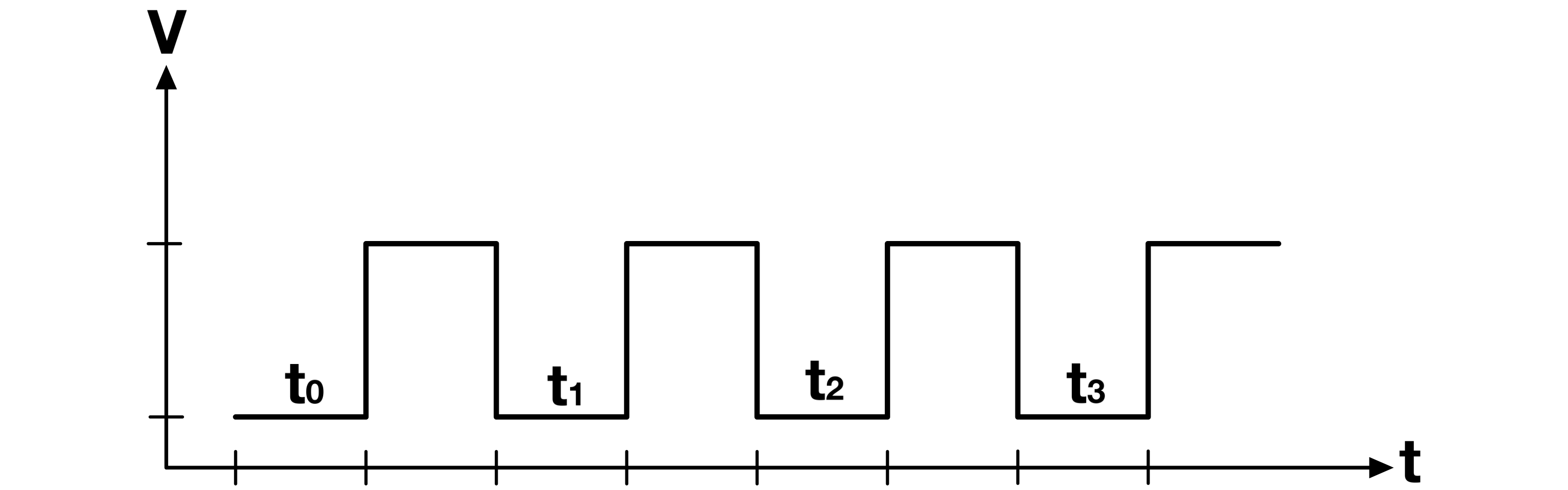
$t_0$: Writes zero into the accumulator and asserts the OLED reset line.
$t_1$: Writes zero into register A, the Bridge Register, and the Instruction Register while continuing to assert OLED reset.
$t_2$: Writes zero into register C and the Flags Register while continuing to assert OLED reset.
$t_3$: Writes zero into the temporary Segmented Display register.
$t_4$: Writes zero into the Segmented Display register and into registers B, D, and E. This step also prepares the shift register with 0b10000000.
$t_5$ to $t_8$: Builds 0xC000 in the Bridge Register by generating 0xC0 and writing it into the high byte of the Bridge Register.
$t_9$: Loads the Stack Pointer with 0xC000.
$t_{10}$: Decrements the Stack Pointer once, so the Stack Pointer starts at 0xBFFF, the top of the lower RAM region.
$t_{11}$: Loads the Program Counter with 0xC000, the start of the bootloader ROM.
$t_{12}$: Toggles the interrupt inhibit state used during reset/startup.
$t_{13}$ to $t_{14}$: All control lines are placed in an inactive state.
$t_{15}$: Fetches the first opcode from 0xC000.
The reset sequence starts by forcing the accumulator to zero, then uses that known zero as the source for clearing several registers. The early reset steps also keep the OLED reset line asserted while the CPU reaches a known state. After the reset sequence builds 0xC000, it initializes the Stack Pointer to 0xBFFF and the Program Counter to 0xC000, which leaves the CPU ready to fetch the first bootloader instruction.
ICs and Logic Parts
1x 74HCT273 Octal D-Type Flip-Flops With Clear (Digikey, Datasheet)
1x 74HCT161, Synchronous 4-Bit Binary Counters, (Digikey, Datasheet)
1x 74HCT14 Hex Schmitt-Trigger Inverters (Digikey, Datasheet)(Shared with Permanent Clock)
1x 74HCT02 Quadruple 2-Input Positive-NOR Gates (Digikey, Datasheet) (Shared with Permanent Clock)
1x 74HCT00 Quad 2 Input NAND Gate (Jameco, Datasheet) (Shared with Permanent Clock)
1x 74HCT154 4-TO-16 INVERTING DECODER, (Jameco, Datasheet)
3x M27C4002 4 Mbit UV EPROM, 256K x 16 organization (Jameco, Datasheet)
1x 74HCT238 3-to-8 non-inverting decoder (Digikey, Datasheet)