Numerical Display Module
Basics Primer
A BCD (Binary-Coded Decimal) decoder is a circuit that converts a binary-coded (binary equivalent) decimal number into a format easily displayed or understood, usually for segmented screens. In BCD, each digit of a decimal number is represented by its binary equivalent.
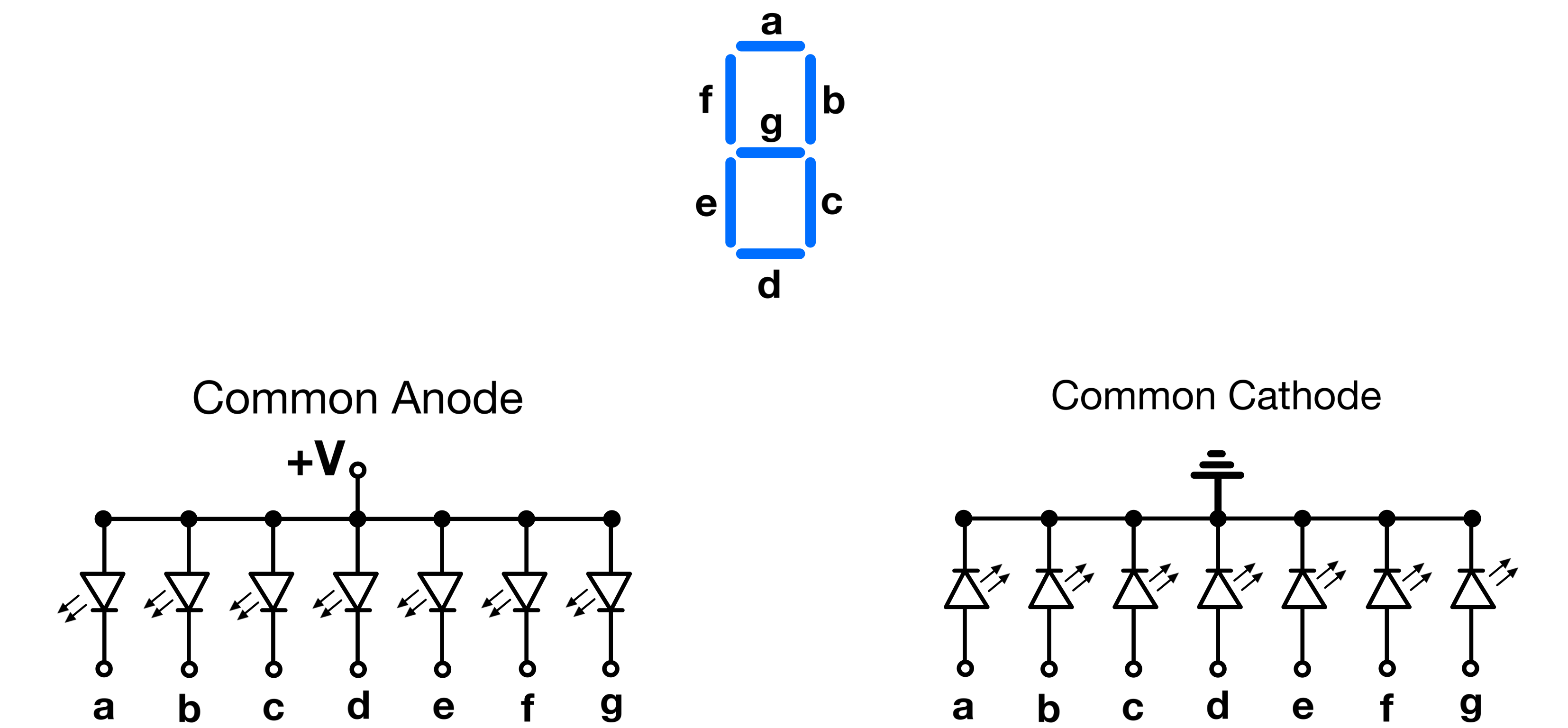
A segment(ed) display is an LED-based numerical display made of individual segments. Each segment illuminates independently to form digits and characters. They usually come in two configurations:
Common Anode: All the anodes of the LED segments are connected together to a common positive voltage. Each segment is powered by grounding its cathode.
Common Cathode: All the cathodes of the LED segments are connected together to a common ground. Each segment is powered by applying a positive voltage to its anode.
The SAP-1 drives four 7-segment displays that can represent all decimal numbers that fit within 8 bits (0 to 255) as well as signed two’s complement (-128 to 127). My display module uses a set of six 14-segment displays that cover all numbers that fit in 16 bits (0 to 65,535), including signed two’s complement (-32,768 to 32,767).
Why Choose a ROM?
Segmented displays can be driven in various ways. Below is an example of one of the simplest methods, in theory, though not the most straightforward in practice:
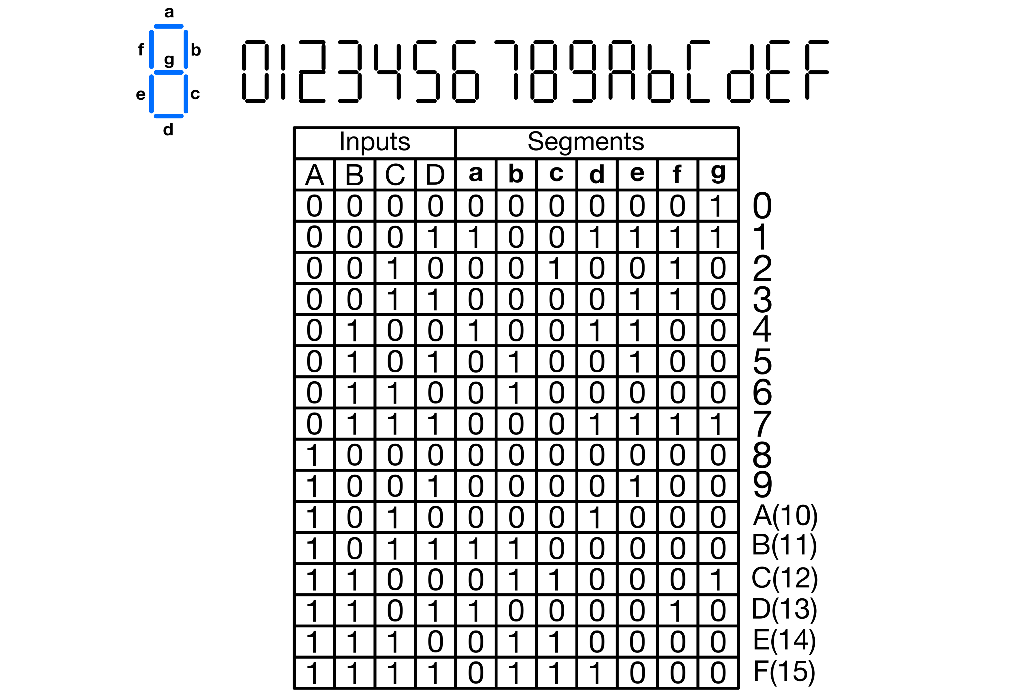
With a 4-bit input, a seven-segment display can show the hexadecimal representation of the input’s 16 possible values. Below is a truth table that outlines the required state for every segment of a common-anode seven-segment display to represent numbers from 0 to 15 in hexadecimal.
The picture below shows a circuit that implements the truth table. Note that besides the NOT gates, all the gates in the implementation below are four-input gates. This means if you only have two-input gates, you need a minimum of three gates per NAND and AND gate shown in the figure.
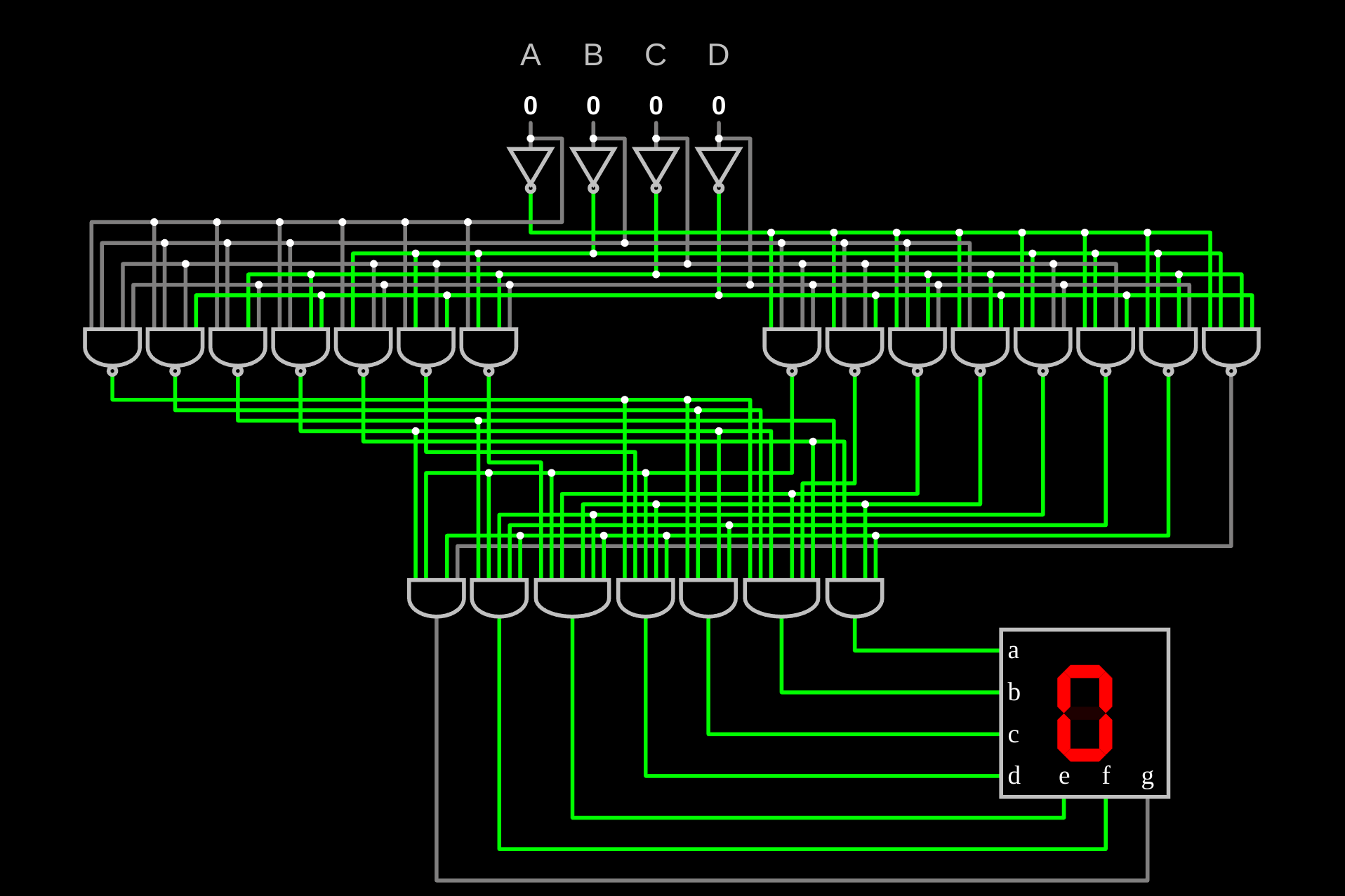
Clearly, the number of gates required to implement the logic for all segments is prohibitive, even when using higher-input gates. A ROM chip, on the other hand, offers a more compact and cost-effective solution because it stores the entire truth table for all segments. ROMs can emulate any combinational circuit because they store their truth tables and act as lookup tables. Instead of building a separate logic network for each segment, the ROM simply stores the desired output pattern for each input code. If the character set needs to change later, only the ROM contents need to change.
Since the display module for the SAP-1 uses four 7-segment displays, a ROM with at least a 22-bit output (3 x 7 bits for the digit displays, and 1 bit for the sign display) can drive all of them. Such a ROM would be relatively expensive, hard to find in through-hole and parallel format, and not easy to program without a dedicated PROM programmer. Another alternative could be the use of a combination of smaller-sized ROMs. For the four displays, four separate ROMs could be used to encode the value for each display individually.
Both of these methods are acceptable, considering their straightforwardness.
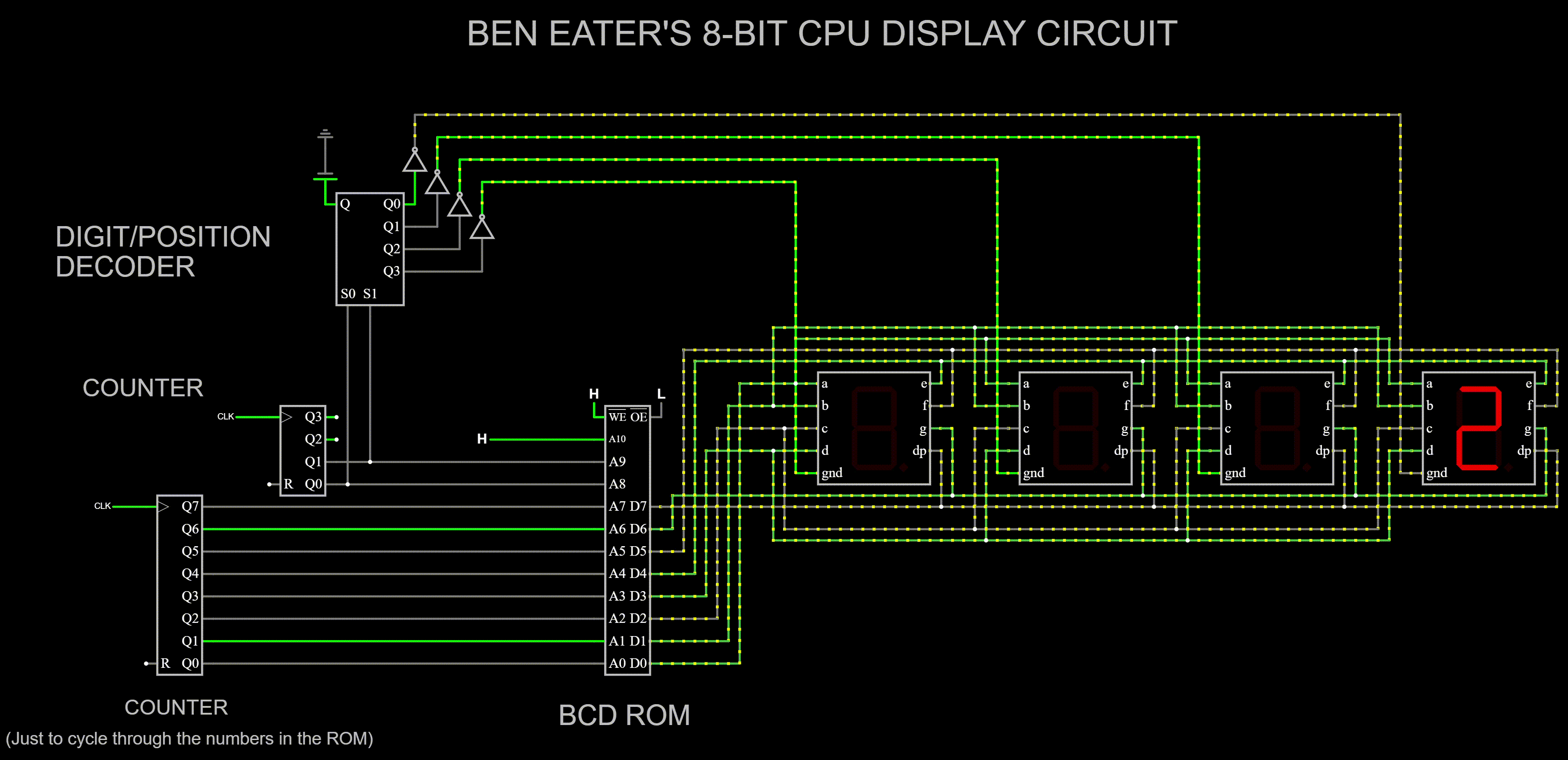
The SAP-1, however, achieves this encoding with only one 16 Kbit ($2Kb×8$) parallel EEPROM, using only 11 address pins and 8 output pins. The clever part of Ben Eater’s display module is that it does not drive all digits independently. Instead, each display activates sequentially, which creates the illusion that all digits appear at the same time. A dedicated clock, binary counter, and decoder handle this selection process. The counter and decoder choose the active display and route the correct EEPROM output to it, while the clock sets how quickly the circuit moves from one display to the next.
I made a Falstad circuit to visualize this process.
This is the highest frequency at which I could run the simulation with a decent recording render. It is just a replica limited by lots of underlying code; the real circuit runs so fast that the switching rate cannot be perceived with the naked eye.
This simulation follows the same logic as the SAP-1’s display module. The bottom left counter is for demo purposes; it is just there to cycle through all the values stored in the BCD ROM. On the actual module, the ROM is driven by the output register. The lower 8 address bits of the ROM are what selects the digit to be displayed, while the next 2 higher address bits are used to select which display the digit must be displayed on. The most significant address bit selects the encoding mode (signed or unsigned).
Note: As of April 1, 2023 (the day I made this simulation), Falstad did not support 14-segment displays nor ROMs with an input address size greater than 15 bits.
Implementation
Control lines involved (4):
- |← ~SE Segmented display enable: Turn ON the display.
- |← SdW Segmented display write: Loads the two 16-bit output register.
- |← SdT Segmented display: Loads the 8-bit output temporary register.
- |← SdM Segmented display Mode: Signed or unsigned.
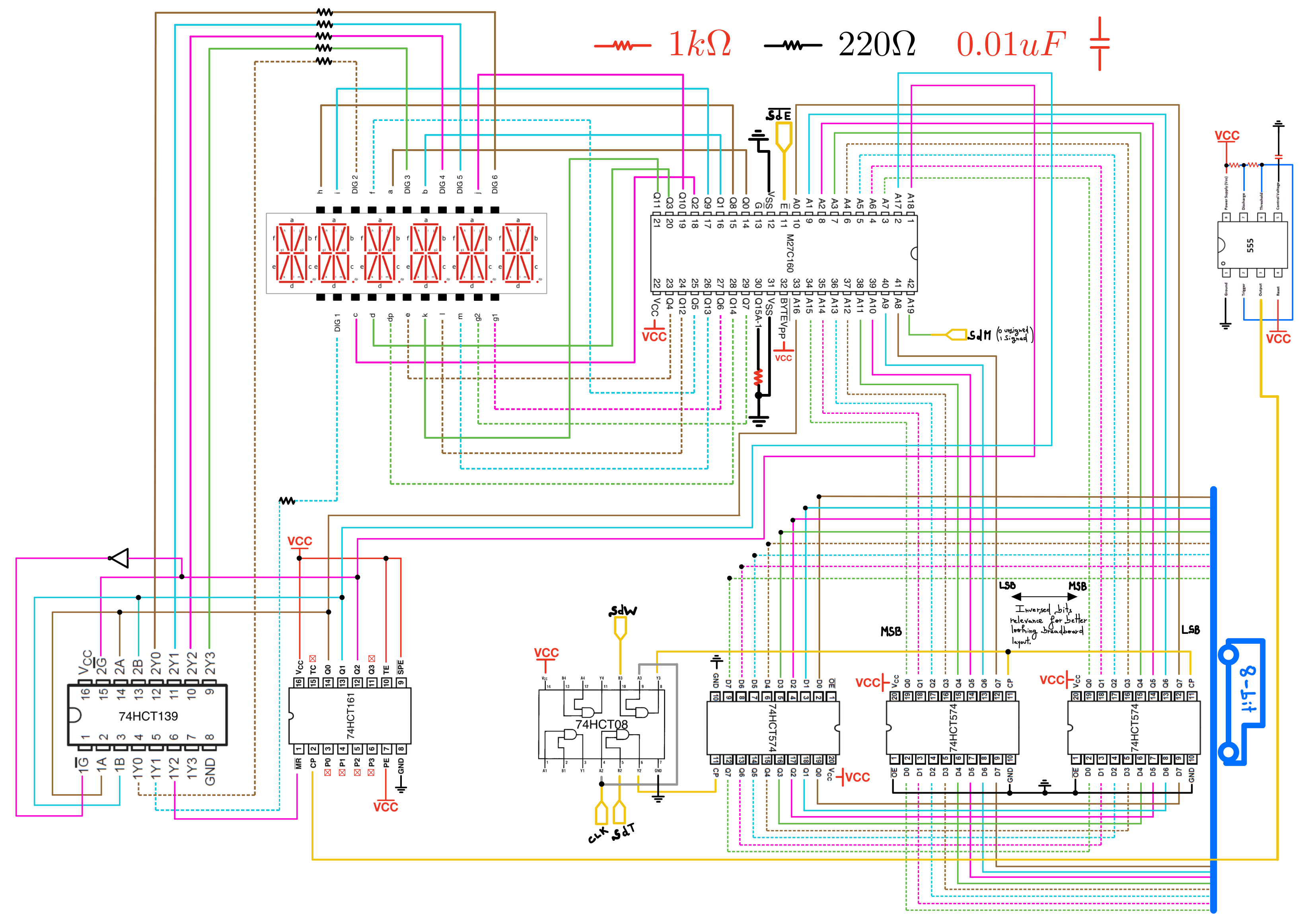
My BCD ROM is an M27C160 16 Mbit UV EPROM, organized as 1M x 16 in word mode. It has 20 address lines, A0 through A19, and 16 data output lines, Q0 through Q15. Similar to the SAP-1 display ROM idea, the lower 16 address bits, A0 through A15, select the 16-bit value being displayed. The next three address bits, A16 through A18, select which of the six display positions is currently active. The most significant address bit, A19, selects the encoding mode: unsigned or signed two’s complement.
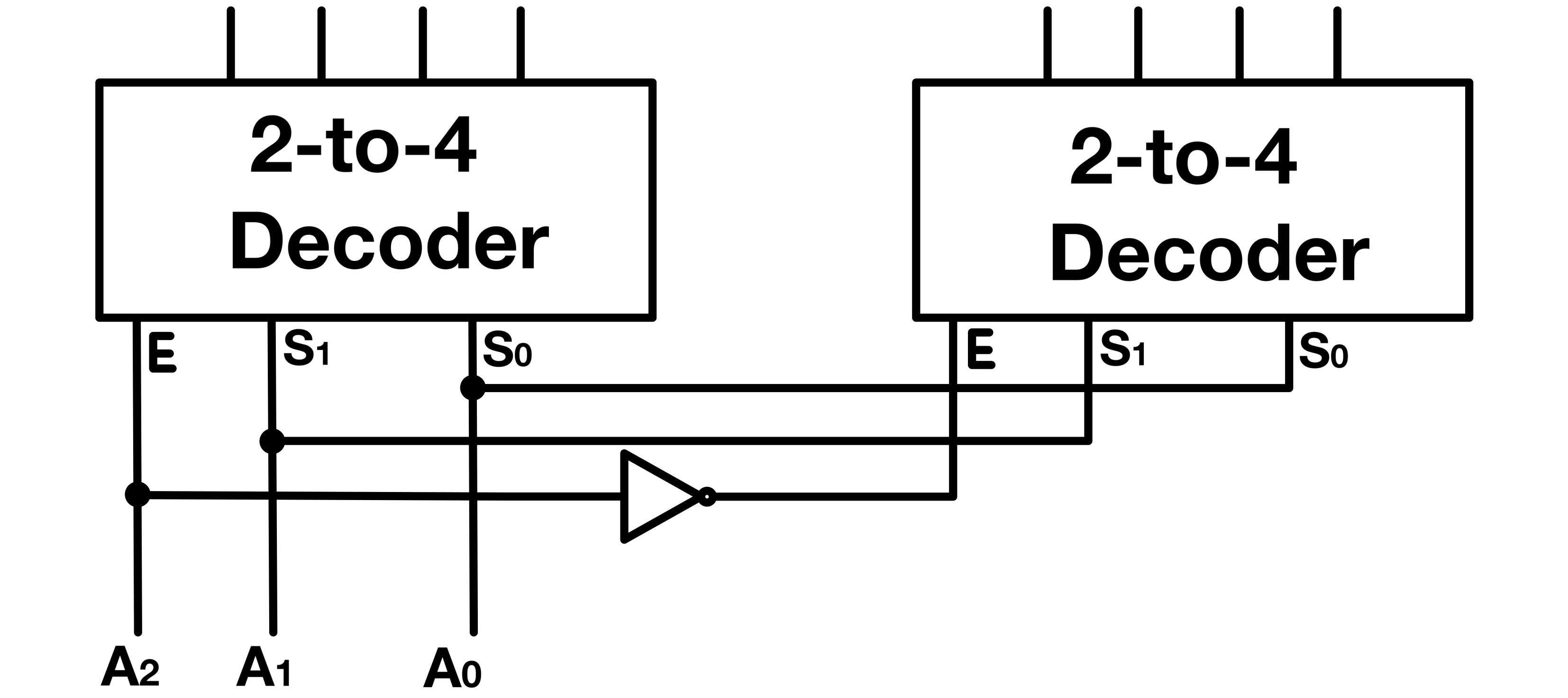
I did not have a 3-to-8 decoder when I built the display module, so I used a 74HCT139 dual 2-line to 4-line decoder to build one. Since the module has six displays, I only need six of the eight decoded output states. I tied the seventh decoded output to the counter’s reset input. This way, after the last display position is selected, the counter resets instead of stepping through the two unused positions.
Output Register
Since my display ROM supports 16-bit numbers, the driving register must output 16-bit values. The output register, however, gets its input from the 8-bit data bus. I use a 16-bit register (made with two 8-bit registers) loaded in two cycles from a temporary register and the data bus.
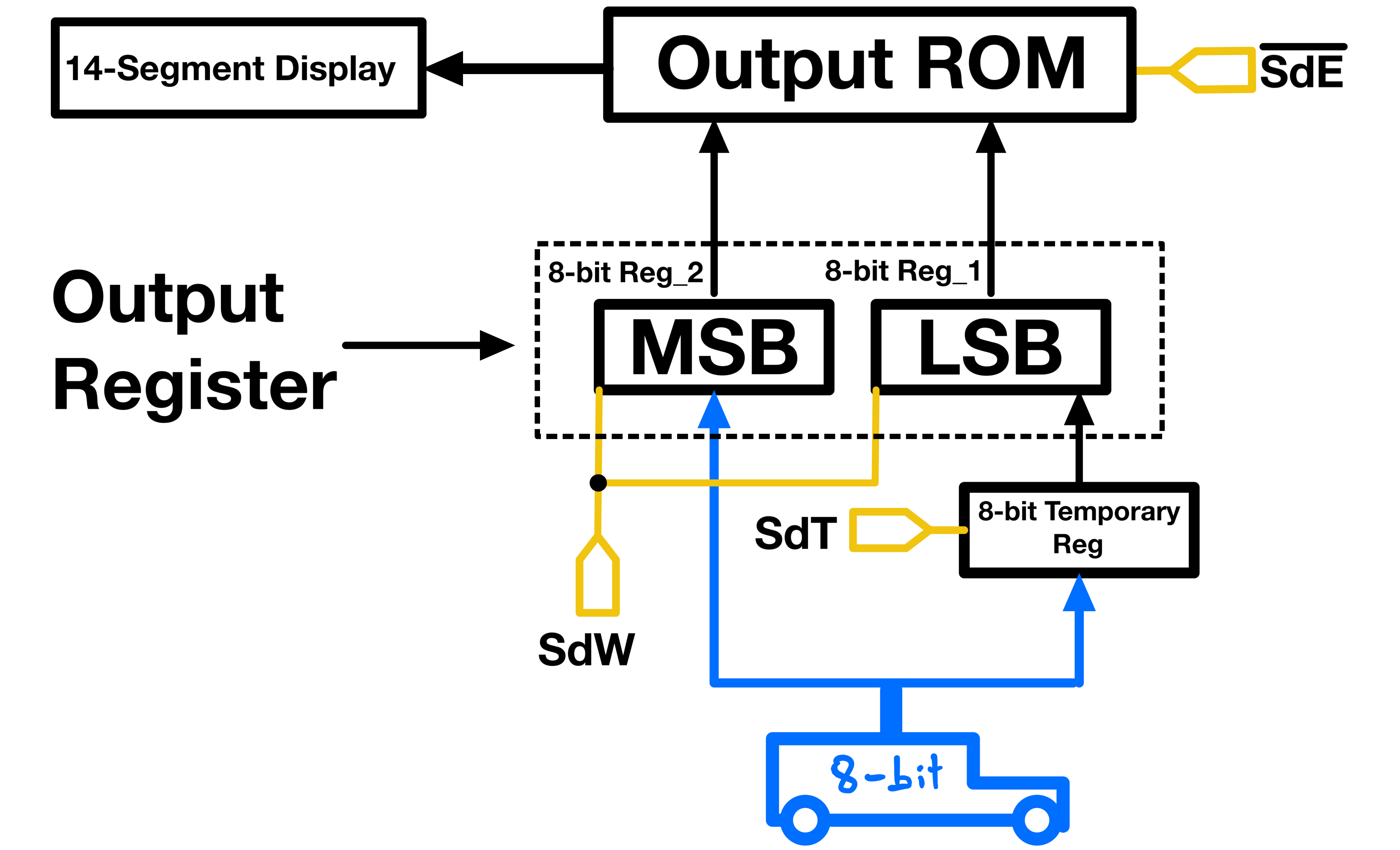
The reason I use three registers(16-bit reg + temp reg) instead of two(just the 16-bit reg) is to keep whatever value being displayed unchanged even through transitions. The output register (Reg_1 + Reg_2) is always outputting to the ROM. In other words its “output enable” is always active.
Assume the display is currently displaying 00000 (0b0000000000000000), meaning Reg_1 and Reg_2 are holding 0b00000000 each.
Now let’s say I want to display 65535 (0b1111111111111111), meaning Reg_1 and Reg_2 must both be loaded with 0b11111111.
With no temporary register, Reg_1 would first be loaded with 0b11111111. At that point, the display would show 00255, because Reg_2 would still be holding 0b00000000. The output register would temporarily contain 0b0000000011111111. Only after an additional cycle would Reg_2 load 0b11111111, and complete the full value.
The temporary register first holds the lower byte, so the display remains at 00000. Then, when Reg_2 receives the upper byte, Reg_1 receives the saved lower byte at the same time. The display then changes from the old 16-bit value to the new value in a single visible step, without any unrelated intermediate value.
BCD CODE
Below is a breakdown of the ROM organization and a Python code generating it:
import array
I’ve experimented with a couple of binary handling libraries to generate ROM images using Python, and I find the “array” module to be the simplest to use.
# Segment patterns for digits on a 14-segment display.
# Modified the patterns for digits 0, 1, and 5.
digits = [0x3f, 0x6, 0xdb, 0x8f, 0xe6, 0xed, 0xfd, 0x7, 0xff, 0xef]
Note: I have a GitHub repository with code and a guide to generate digits and character patterns(ROM outputs) for different types of segmented displays.
# Opening/Creating the output file in binary mode to save ROM's image.
doc = open('rom1.bin', 'wb')

# Constants for the ROM's output mode and the ROM size.
OUTPUT_WORD_SIZE = 16
ROM_SIZE = 2**OUTPUT_WORD_SIZE

# Number of digits used, excluding sign digit.
DISPLAY_DIGITS = 5

# Deducting the number of unused states.
DECODER_SELECTS = 3
UNUSED_STATES = 2**DECODER_SELECTS - (DISPLAY_DIGITS + 1)

# Start address for unsigned numbers.
UNSIGNED_START = 0

# Start and end addresses for the sign of unsigned numbers.
UNSIGNED_0_START = UNSIGNED_END = ROM_SIZE*DISPLAY_DIGITS
UNSIGNED_0_END = UNSIGNED_0_START + ROM_SIZE

# Calculates the size to fill unused addresses with zeros.
FILL = ROM_SIZE*UNUSED_STATES

# Start and end addresses for the complements of numbers.
COMPLEMENT_START = UNSIGNED_0_END + FILL
COMPLEMENTS_SIGN_START = COMPLEMENT_END = COMPLEMENT_START + (ROM_SIZE*DISPLAY_DIGITS)
COMPLEMENTS_SIGN_END = COMPLEMENTS_SIGN_START + ROM_SIZE
ROM Organization
1- Addresses 0 to 393216 (First Half):
This half of the ROM is divided into six sections, each corresponding to one of the six displays. Each section has 65536 addresses:
1’s place: addresses 0 through 65,535
10’s place: addresses 65,536 through 131,071
100’s place: addresses 131,072 through 196,607
1000’s place: addresses 196,608 through 262,143
10000’s place: addresses 262,144 through 327,679
Sign place: addresses 327,680 through 393,215
The signs place is the 6th tick of the counter(6 * 65,536 = 393,216).
Note:
"H"inwrite(array.array("H", []))stands for unsigned short integers (Usually 2 bytes in most systems). It specifies the type of data that the array will hold.# Writes data for unsigned numbers. for i, index in enumerate(range(UNSIGNED_START, UNSIGNED_END, ROM_SIZE)): print(f"{10**i}'s place, from {index:,} to {index+ROM_SIZE:,}") for x in range(ROM_SIZE): doc.write(array.array("H", [ (digits[x % 10] if i==0 else digits[\ int(x / (10**i))% 10])] ))The data in these sections represents unsigned numbers, with each section corresponding to a different place value in a decimal number (units, tens, hundreds, etc.).
  # Writes data for the sign place of unsigned numbers.
  print(f"signs place, from {UNSIGNED_0_START:,} to {UNSIGNED_0_END:,}\n")
  for x in range(ROM_SIZE):
    doc.write(array.array("H", [0x0]))
2- Addresses 393216 to 458,752 to 524288 (Middle Section):
This area is a buffer zone between the sections for unsigned numbers and their complements. It is unused and filled with zeros.
  # Fill unused addresses with zeros.
  print(f"Filling {UNSIGNED_0_END:,} to {UNSIGNED_0_END + FILL:,}\
  (unused addresses) with zeros\n")
  for x in range(FILL):
    doc.write(array.array("H", [0x0]))
3- Addresses 524288 to 917504 (Second Half):
This section is also divided into six segments, each with 65536 addresses.
  # Writes data for the complements of numbers.
  for i, index in enumerate(range(COMPLEMENT_START, COMPLEMENT_END, ROM_SIZE)):
    print(f"Complements {10**i}'s place, from {index:,} to {index+ROM_SIZE:,}")
    for x in range(-(int(ROM_SIZE/2)), (int(ROM_SIZE/2))):
      doc.write(array.array("H", [ (digits[abs(int(x/(10**i))) % 10]) ]))
These segments store the complements of the numbers. The data represents the negative values of the corresponding positive values in the first half. The signed two’s-complement section is selected by the SdM control line connected to A19.
  # Writes data for the sign place of complements.
  print(f"Complements signs place, from {COMPLEMENTS_SIGN_START:,} to \
  {COMPLEMENTS_SIGN_END:,}")
  for x in range(-(int(ROM_SIZE/2)), (int(ROM_SIZE/2))):
      if x < 0:
          doc.write(array.array("H", [0xc0]))
      else:
          doc.write(array.array("H", [0x0]))
Just like in the first half, each segment represents a different place value.
4- Addresses 917504 to 1048576 (End Section):
This final section, like the middle one, is unused and filled with zeros. It fills the remainder of the ROM to make the binary image file size equal the ROM’s actual size.
  # Fills remaining unused addresses with zeros.
  print(f"Filling {COMPLEMENTS_SIGN_END:,} to {COMPLEMENTS_SIGN_END + FILL:,}\
  (unused addresses) with zeros\n")
  for x in range(FILL):
    doc.write(array.array("H", [0x0]))

  doc.close()
This code is also available on my GitHub.
ICs
1x M27C160-100F1 16 Mbit UV EPROM, 1M x 16 organization (Datasheet)
1x LMC555CN CMOS Single 555 Timer Low Power (Jameco, Datasheet)
1x 74HCT161, Synchronous 4-Bit Binary Counter, (Digikey, Datasheet)
2x 74HCT245, octal bus transceivers with 3-state outputs, (Digikey, Datasheet)
1x Common-Cathode 6-digits 14-segment display, (Alibaba)
1x 74HCT139 Dual 2-Line To 4-Line Decoders/Demultiplexers (Digikey, Datasheet)