RAM & ROM Primer
Before the RAM module, I want to introduce a few memory concepts that appear often in digital electronics. Some of these details go beyond what this build strictly needs, but after the RAM section, they may feel more intuitive and easier to connect to real hardware.
Basics Primer
Random Access Memory
Random access memory (RAM) allows data to be read from or written to any memory location in roughly the same amount of time, regardless of where that data physically sits inside the chip. Most RAMs are volatile: they only keep data as long as the device has power. Data is lost when power is cut off. The main difference between volatile and non-volatile memory is the process used to hold data. Non-volatile storage technologies use different physical mechanisms to retain data without power. These mechanisms typically increase read and/or write time compared to volatile RAM.
Volatile random-access semiconductor memory comes in two main forms: static random-access memory (SRAM) and dynamic random-access memory (DRAM).
DRAM
DRAM is commonly used as the main memory in computers because it offers a good balance between cost and storage capacity. It works by storing bits within memory cells: These cells, in their most basic form, consist of a capacitor paired with a transistor. When the circuit needs to store or retrieve a bit, the transistor charges or discharges its paired capacitor. A charged capacitor corresponds to a “1” while a discharged capacitor corresponds to a “0”. These charges and discharges are controlled by two lines: the wordline and the bitline, which are just “wires” connecting to nodes within the memory array.
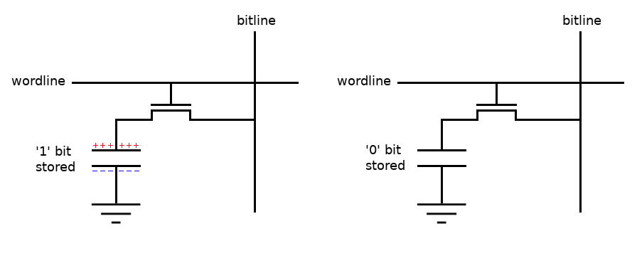
In DRAM, reading data is a destructive process because accessing the cell disturbs the stored charge. The sense amplifier detects the small voltage change and restores the value after the read. Pre-charging prepares the bitlines for the next access. Additionally, DRAM capacitors leak charge over time, so the system must refresh the cells periodically. This need for refresh is what gives DRAM its “dynamic” characteristic.
As more memory cells are packed into a given area, each cell has less space. The capacitors become smaller, hold less charge, and become harder to read directly. For this reason, a sense amplifier detects the minor variations in charge to read a cell’s content, then outputs the corresponding logic level.
SRAM
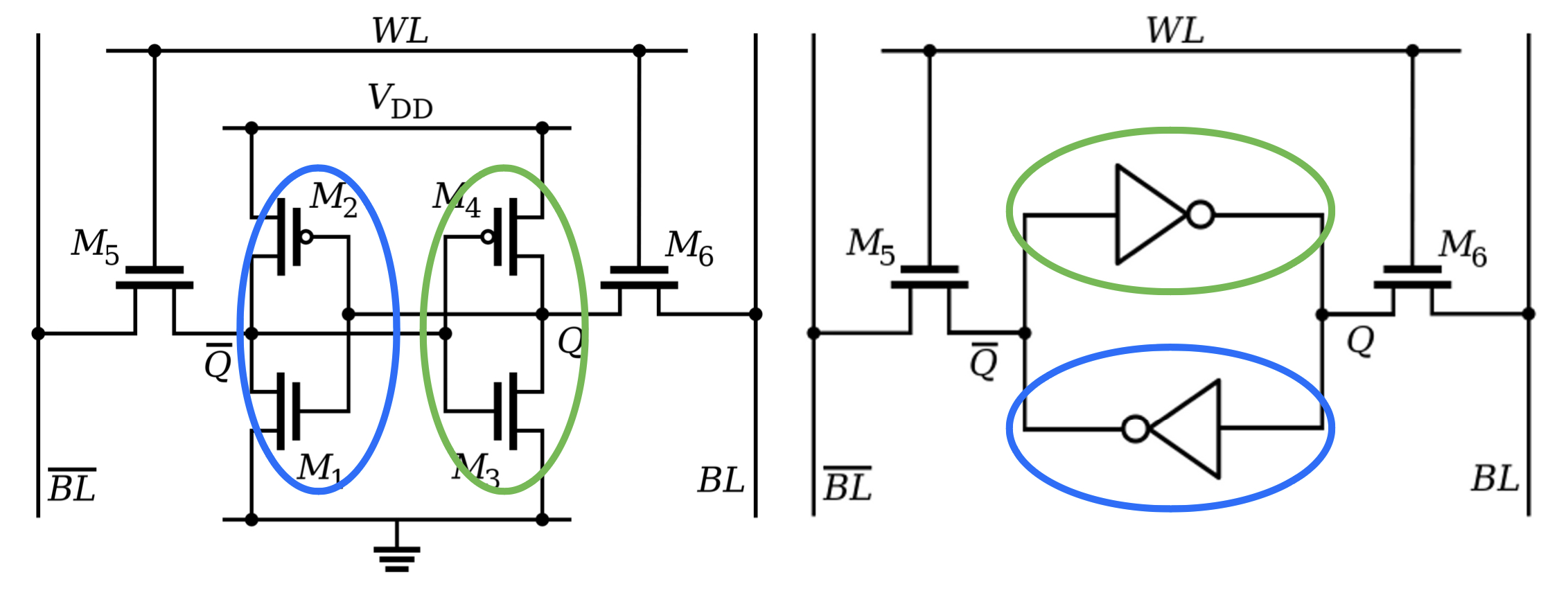
Unlike DRAM, a typical SRAM cell uses two cross-coupled inverters and two access transistors. The cell does not rely on stored capacitor charge, so it does not need periodic refresh. However, SRAM still requires power to preserve its data, so it is volatile.
SRAM is faster than DRAM, so it serves well as cache memory. However, because it uses more transistors per bit of memory, it is more expensive and less dense compared to DRAM. As a result, SRAM is not typically used for main processor memory. For a breadboard CPU, however, SRAM is much easier to use than DRAM because it does not require refresh circuitry.
Both DRAM and SRAM organize their memory in a matrix of rows and columns, controlled by integrated address decoders.

SRAM is “static” because its cross-coupled inverters hold the stored bit state as long as power remains applied. My CPU uses SRAM because it is much easier to work with on a breadboard than DRAM: it is relatively cheap, fast enough for this build, and does not require refresh circuitry.
Figure 3 shows how the pairs (M1, M2) and (M3, M4) each form a CMOS inverter.
SRAM operates in three primary modes: hold, read, and write:
Hold State: In this state, the word line “WL” is set to 0, which turns OFF transistors M5 and M6. As a result, the state of the internal latch, which holds the bit value, remains unchanged. This is how the cell retains its data when not actively read or written.
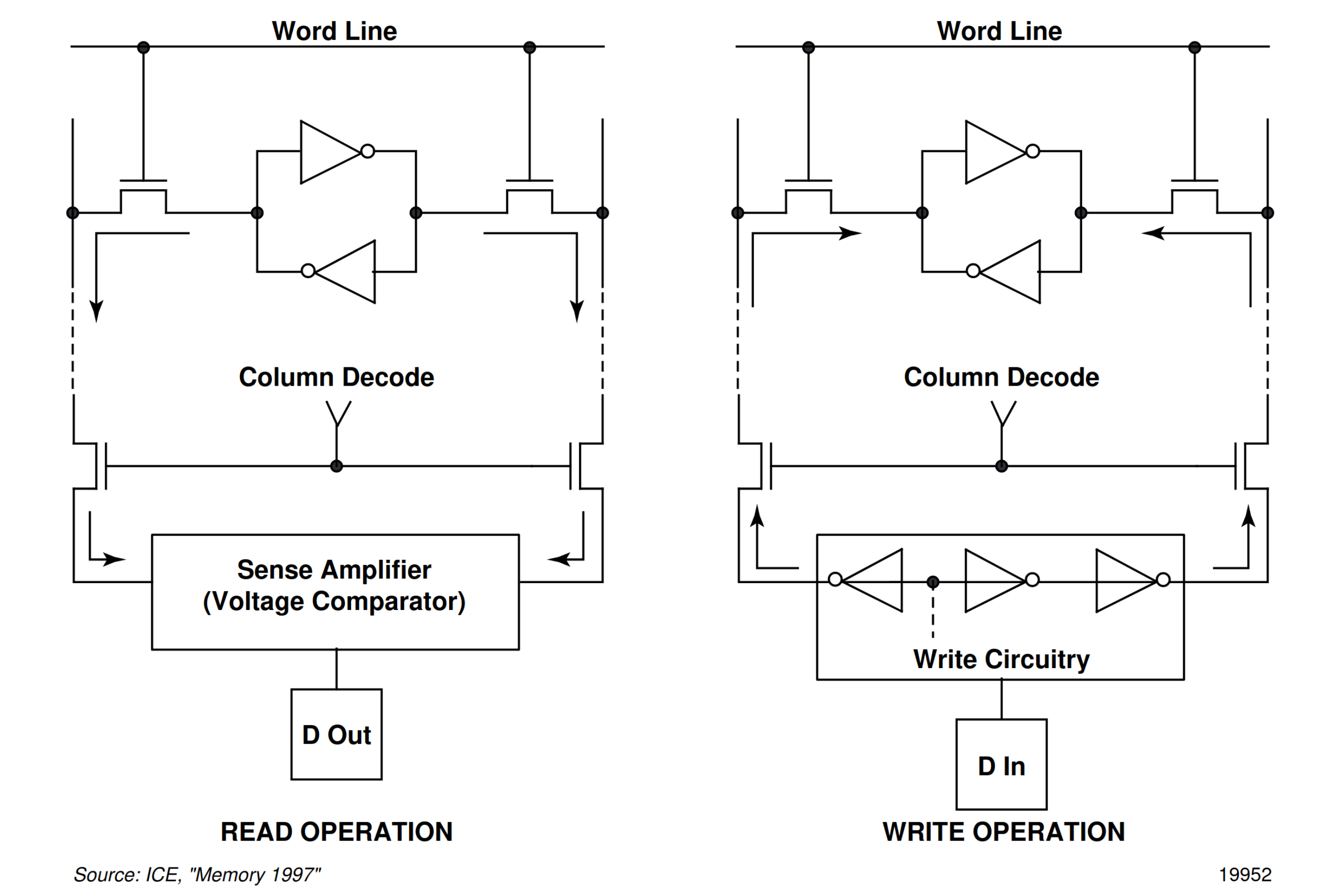
Read Operation: During a read operation, the address decoder activates the word line. M5 and M6 turn on, which connects Q and ~Q to their respective bit lines. The sense amplifier connected to the bit lines detects whether the cell stores a logic 1 or 0. The result then passes to the output buffer and finally to the output pad. A typical memory system has one sense amplifier per output pad.
Write Operation: For writing data, a similar process is initiated. The address decoder activates the word line. The new data, which is to be stored, is then provided through the sense/write circuit. The bit values on the bit lines are overwritten by this new data. During this process, the drivers in the write circuitry, which are stronger than the cell’s flip-flop transistors, force the new data onto the cell, to update its stored state.
Memory Array
Generally, RAM cells, or bitcells, are grouped into arrays. Specific locations are accessed using row and column decoding. At a high level, the address selects a storage location, then the memory chip either reads data from that location or writes new data to it.
In DRAM, memory cells are organized into larger structures such as rows, columns, banks, and, at the module level, ranks. DDR stands for Double Data Rate, which means data can transfer on both the rising and falling edges of the clock signal.
A memory rank is a group of DRAM chips on a memory module that are selected and accessed together. Ranks mainly help increase the capacity of a memory module. In some systems, multiple ranks can also help memory bandwidth because the memory controller may prepare or refresh one rank while another rank is being accessed, depending on the controller and memory organization.
For this CPU project, the important idea is simpler: memory is selected by an address, and the CPU uses the address bus and data bus to read from or write to that selected location.
ROM
ROM stands for Read-Only Memory, and unlike RAM, ROM is characterized by its non-volatile nature. This means that the data stored within ROM chips doesn’t disappear when power is cut off. ROM serves as a foundational memory type in computers and many electronic devices.
ROM is commonly used to store essential data that should not change during normal operation, such as firmware or software required for the device to function. For instance, ROM is often used to store the boot instructions that a computer follows when powering up, such as conducting system checks and loading the operating system into RAM.
Types of ROM
While traditional ROM was strictly read-only, over time, more flexible variations have become available:
- PROM (Programmable Read-Only Memory): This is a type of ROM that can be programmed once after manufacturing. Once programmed, its data becomes permanent.
- EPROM (Erasable Programmable Read-Only Memory): Can be reprogrammed and can be erased using strong ultraviolet light.
- EEPROM (Electrically Erasable Programmable Read-Only Memory): This more modern variation allows data to be electrically erased and rewritten, which makes it more flexible.
- Flash Memory: (Yes! Flash is a type of ROM) A type of EEPROM that erases or writes to multiple areas in one operation. It is widely used in USB drives, memory cards, and solid-state drives.
ROM in Modern Computing
In modern computers, boot firmware such as BIOS or UEFI is stored in non-volatile memory. At power-up, that firmware initializes the hardware and starts the process of loading the operating system from storage into RAM.