Overview
In November 2022, I bought Ben Eater’s 8-bit breadboard CPU kit after seeing one of his Black Friday posts. I had followed his channel for a while, and his computer architecture videos were a major reason I wanted to build a CPU at an IC/macro level.
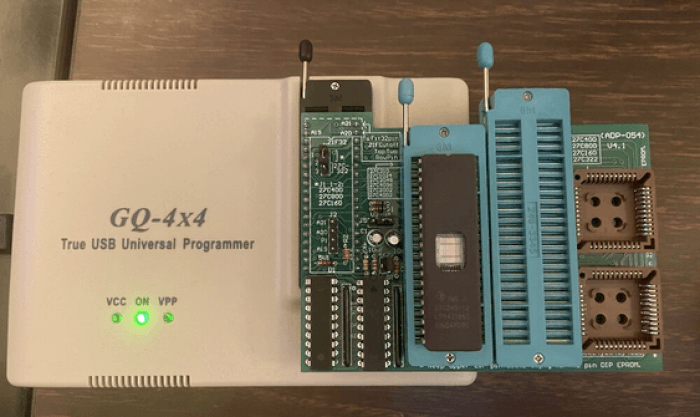
Project repository: All related project files are available on GitHub: F8-BB 8-bit breadboard CPU repository.
Ben’s CPU is based on the SAP-1 (Simple as Possible 1) architecture, as outlined in Digital Computer Electronics by Albert Malvino and Jerald Brown. I built the kit during Spring 2023, then rebuilt parts of it, experimented with more RAM, and eventually started building a larger version of the machine. This series documents that expanded build.
Before going further, I want to give proper credit to Ben Eater. This project started from the foundation he made approachable through his videos and kit. I see this build as another path through the same family of SAP-style ideas, with added hardware and software that fit what I wanted to explore.
Der_ULF1’s 8-bit CPU series also influenced parts of my design, especially the interrupt handling, I/O work, and PS/2 module. His implementation matched several ideas I had in mind and pushed them further. His GitHub is here, and his YouTube channel is here.
While working on the build, I spent a lot of time reading posts on the unofficial Ben Eater subreddit, r/beneater. It is a useful community for seeing other builds and getting feedback from people working through similar problems.
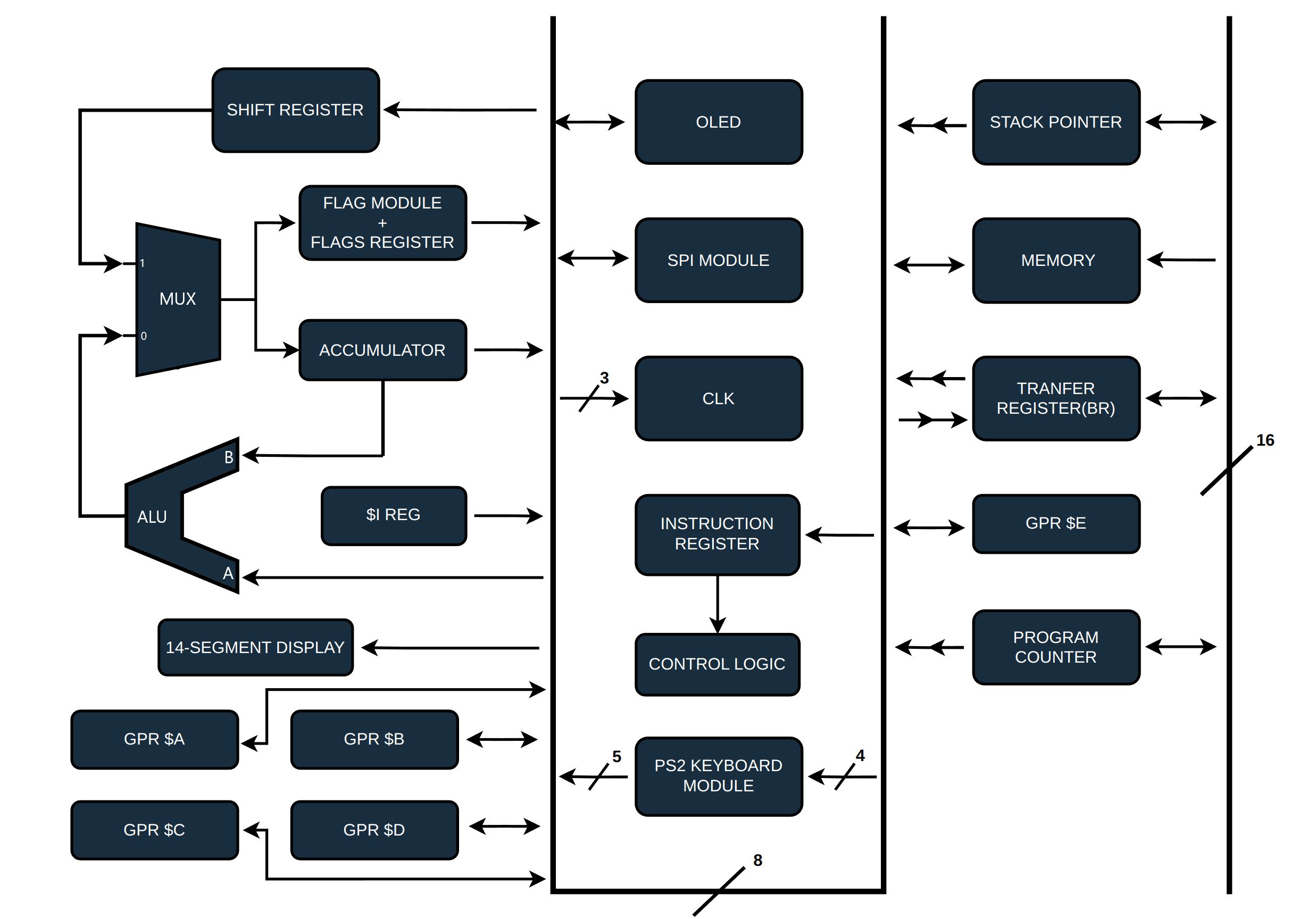
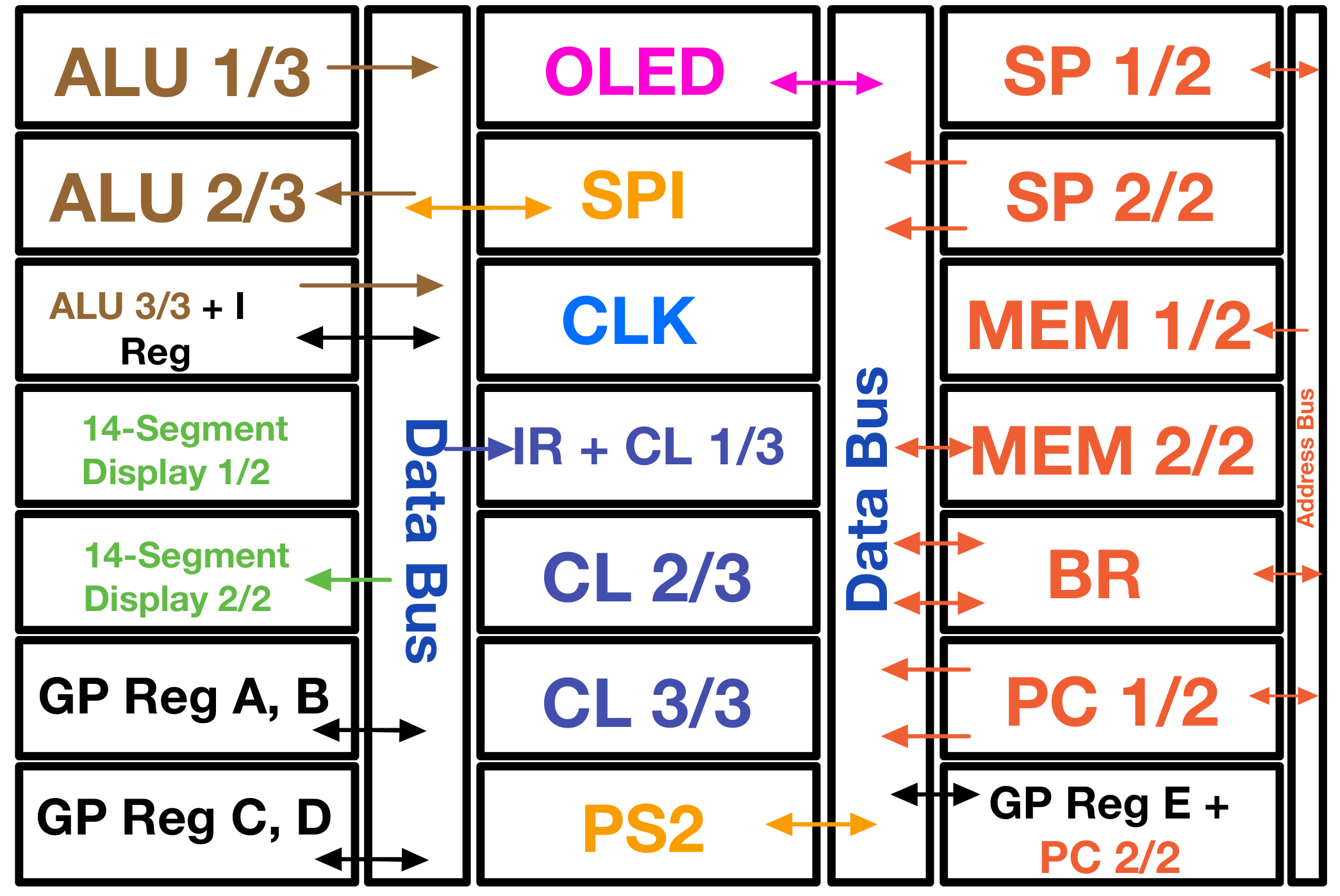
Digital Computer Electronics describes three simplified Von Neumann architectures: SAP-1, SAP-2, and SAP-3. Each one adds more capability than the previous one. My build leans toward the SAP-3, with an 8-bit data bus and 16-bit system/address bus, plus additional hardware for memory, I/O, display output, and software-controlled behavior.
The original SAP-1 is intentionally small: it has a 4-bit program counter, 16 bytes of RAM, and a compact instruction set. That simplicity makes it excellent for learning, but it also limits the programs it can run. My version keeps the same educational spirit while expanding the machine into a larger microcoded CPU with more memory, stack support, I/O, and display hardware.
Notable features of the build:
- Programmable clock speed with eight selectable clock rates.
- 8-bit data bus and 16-bit system/address bus.
- 16-bit program counter.
- 16-bit stack pointer.
- Bridge register for transfers between the 8-bit data bus and 16-bit system bus.
- 48 KB of directly mapped RAM, a bootloader ROM window from
0xC000through0xFFFF, and a downward-growing stack initialized at0xBFFF. - Microcoded control unit.
- 4-bit microcode step counter with dynamic step reset.
- ALU support for ADD, SUB, AND, OR, XOR, LSL, and LSR.
- ALU flags for zero, overflow, negative, and carry.
- Five general-purpose registers: A, B, C, D, and E, with E used as a partial GPR.
- 16-bit numerical output register.
- Multi-digit 14-segment numerical display.
- 128 x 64 monochrome OLED display.
- SPI bus for external peripherals such as an SD card interface.
- PS/2 keyboard decoder.
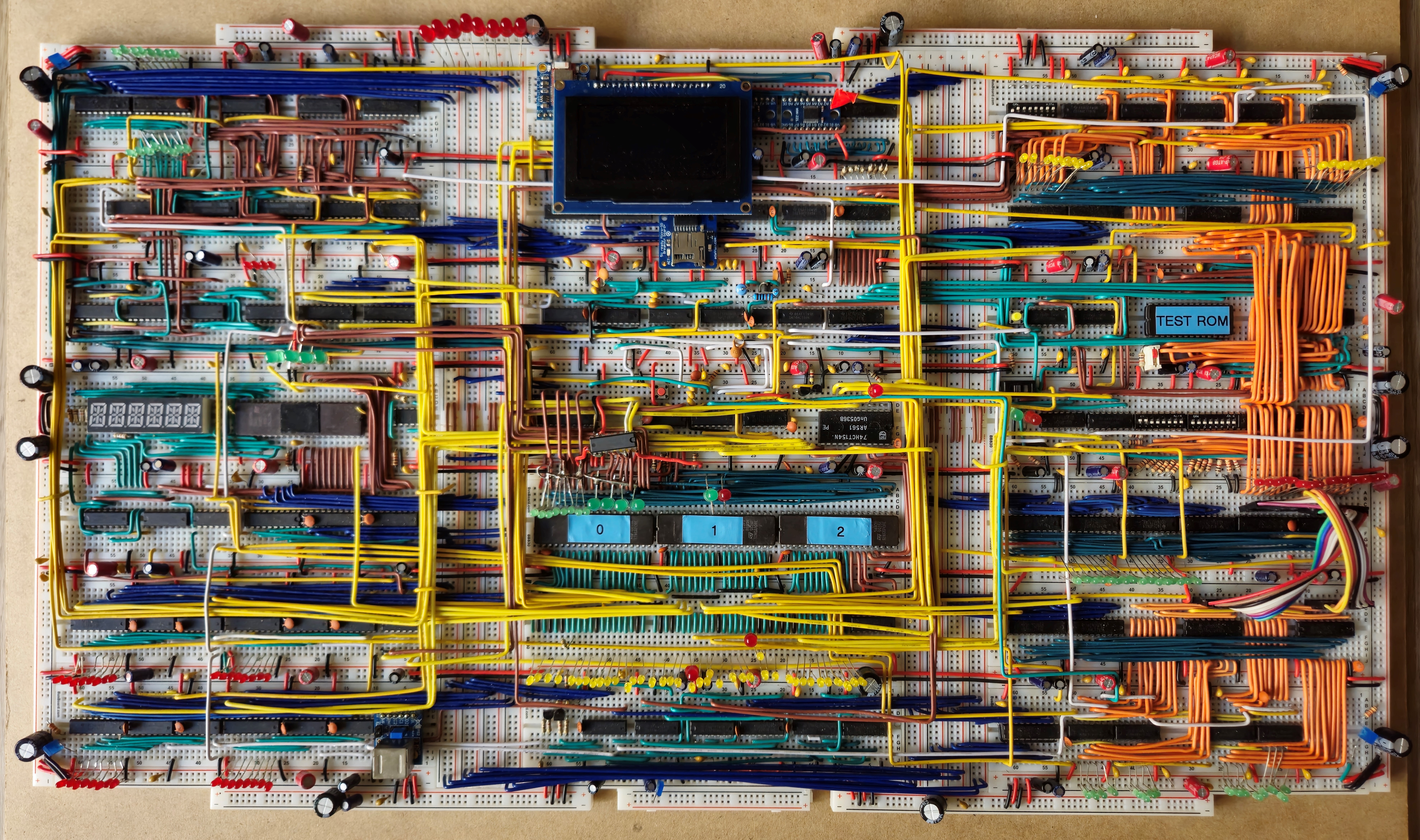
Below is a layout view of every breadboard’s contents.
The build uses mostly 74HCT logic, with a few other logic families where needed. Since the machine uses a large number of ICs on breadboards, power distribution, bypass capacitors, and wiring discipline became important parts of the build.
The complete project repository is available on GitHub: F8-BB 8-bit breadboard CPU repository.