RAM & Transfer Register
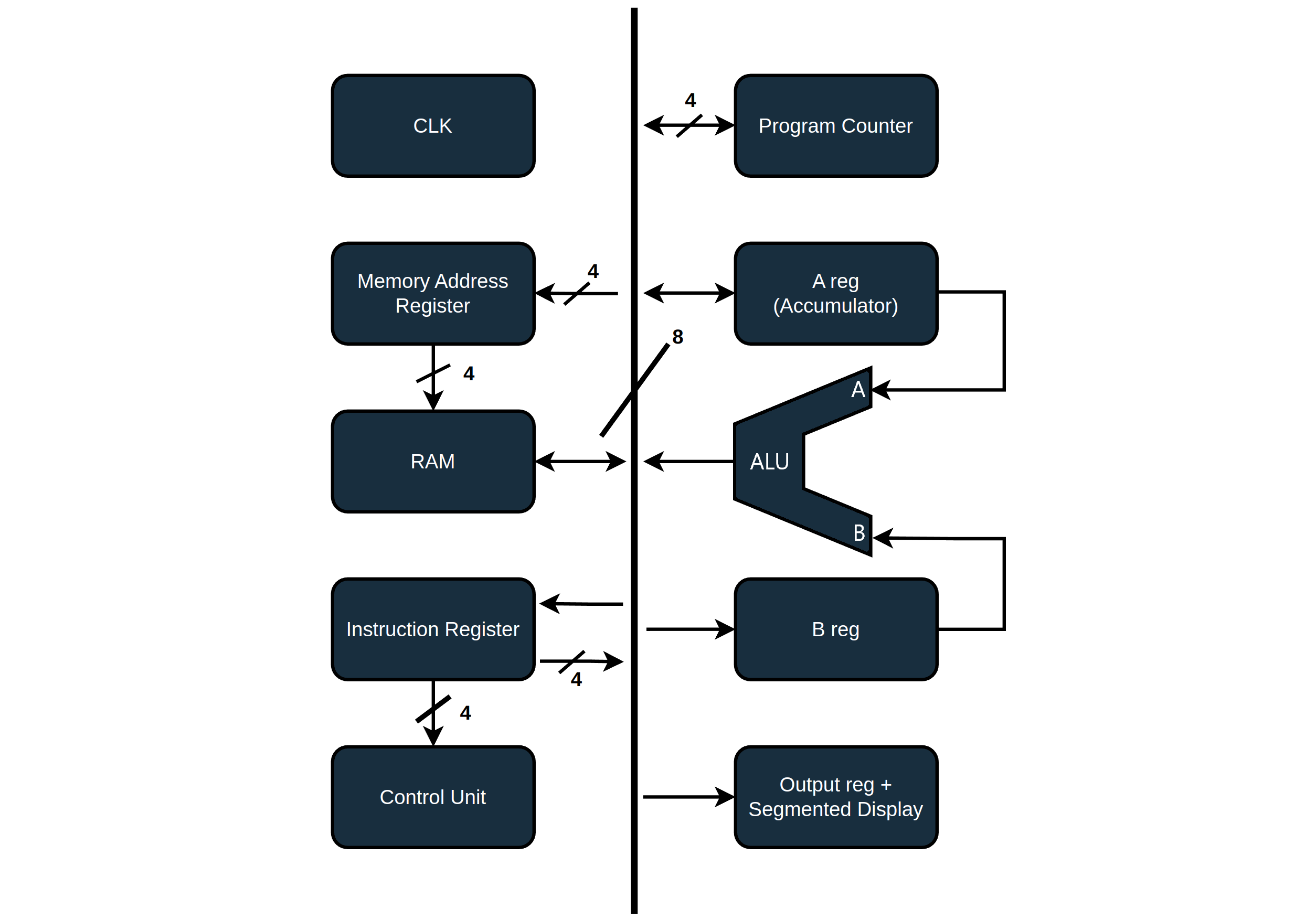
To fetch addresses coming from the Program Counter (PC), the SAP-1 uses a Memory Address Register (MAR) to first store the addresses before accessing them in RAM. My build has no need for a MAR, as it has a dedicated memory/system bus. With a system bus, the PC and all other memory-related modules interface with the RAM and each other directly.
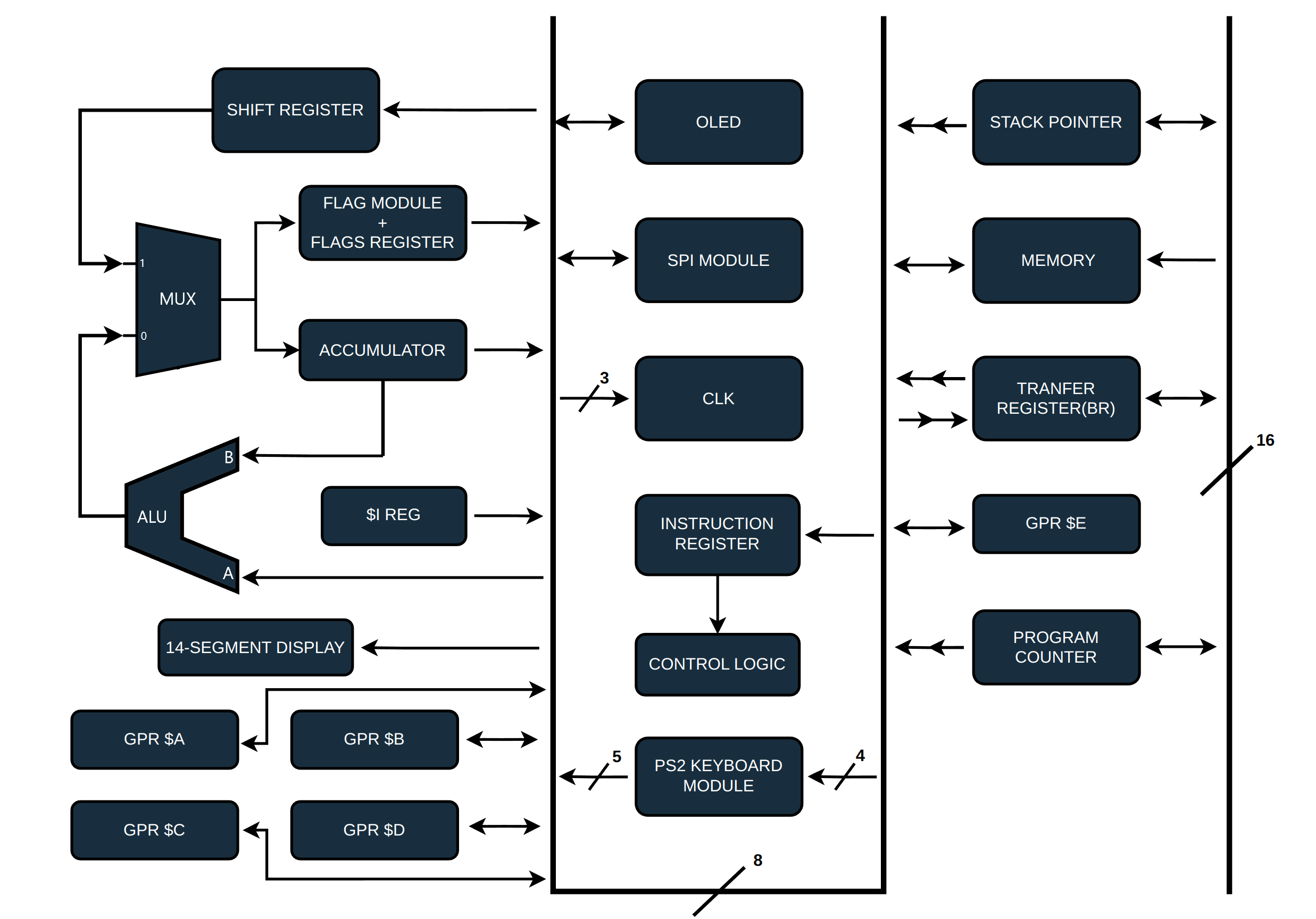
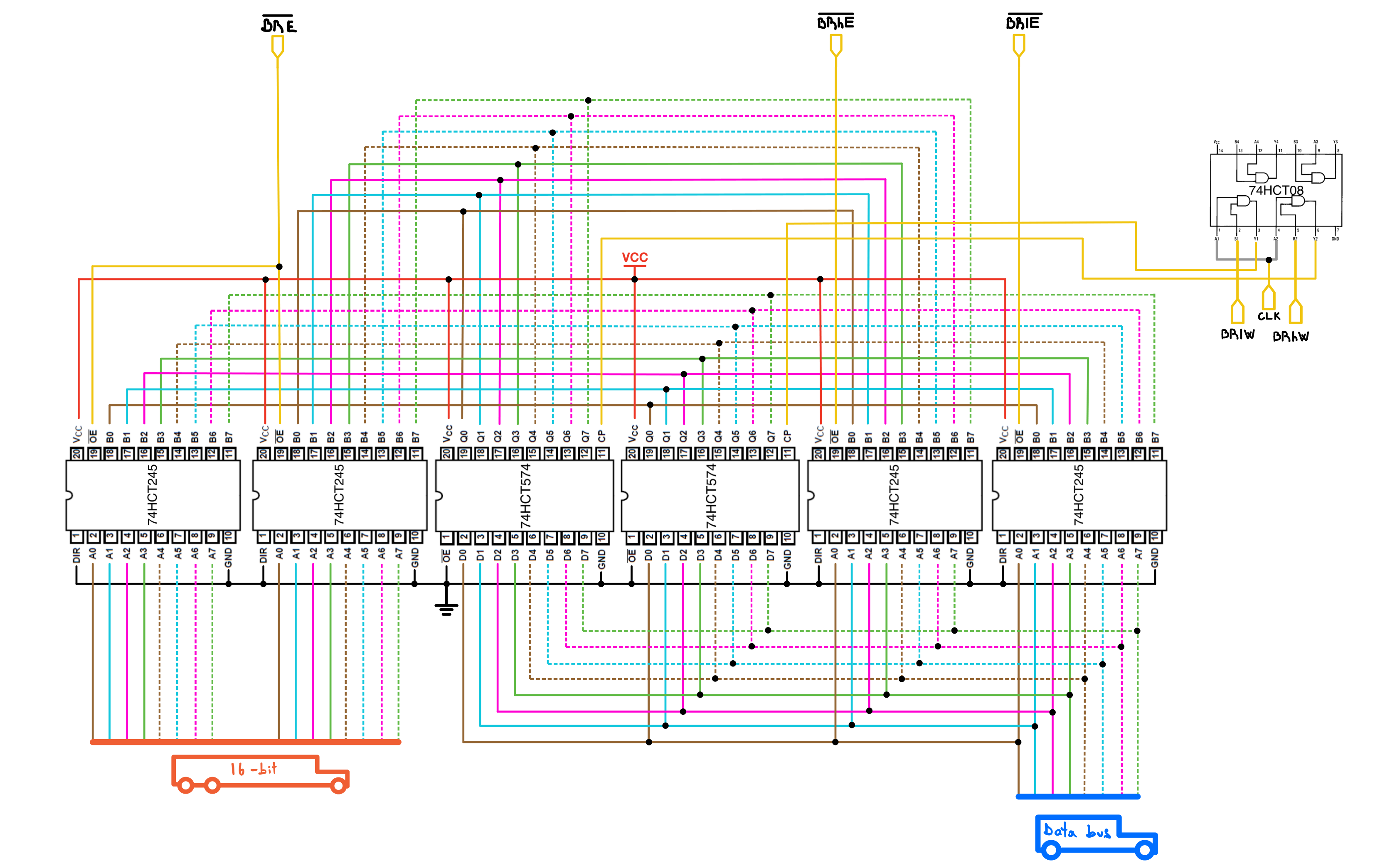
The transfer register, which I call the BR (Bridge), is a 16-bit register that moves data between the 8-bit data bus and the 16-bit system/memory bus in two cycles. The CPU can’t directly read from the data bus into the 16-bit special registers, except for the Segmented Display (SD) register. In my programs, I use little endian to load values into the BR, which is really just an arbitrary preference over big endian. Endianness refers to the order in which bytes are arranged. In little endian, the least significant byte is stored first, while in big endian, the most significant byte comes first. Endianness doesn’t change the computer’s performance; it’s just a different way of organizing data.
Implementations
Transfer Register
Control lines involved (5):
- |← ~BRE Bridge Enable: Enables the address bus to the transfer register’s input.
- |← BRlW Bridge Lower Write: Writes data from the data bus to the lower byte of the transfer register.
- |← BRhW Bridge Higher/Upper Write: Writes the content on the data bus to the upper byte of the transfer register.
- |← ~BRhE Bridge Higher/Upper Enable: Enables the upper byte of the transfer register to the data bus.
- |← ~BRlE Bridge Lower Enable: Enables the lower byte of the transfer register to the data bus.
The transfer register consists of a 16-bit register made with two 8-bit 74HCT574. The 574’s layout turned out to be extremely convenient for this module because the large amount of jumper wires are evenly spread on both sides of the breadboard. Like every module interacting with the address bus, it has two pairs of transceivers. One transceiver pair lets the 16-bit system bus drive the BR input path when ~BRE is active. The other side interfaces the BR with the 8-bit data bus, so the lower and upper bytes can be written or read separately with BRlW, BRhW, ~BRlE, and ~BRhE.
RAM
Control lines involved (3):
- |← ~SPE Stack Pointer Enable: selects the stack/RAM path in the upper address range when LOW; allows ROM selection when HIGH.
- |← ~ME Enables memory output to the data bus.
- |← ~MW Memory write.
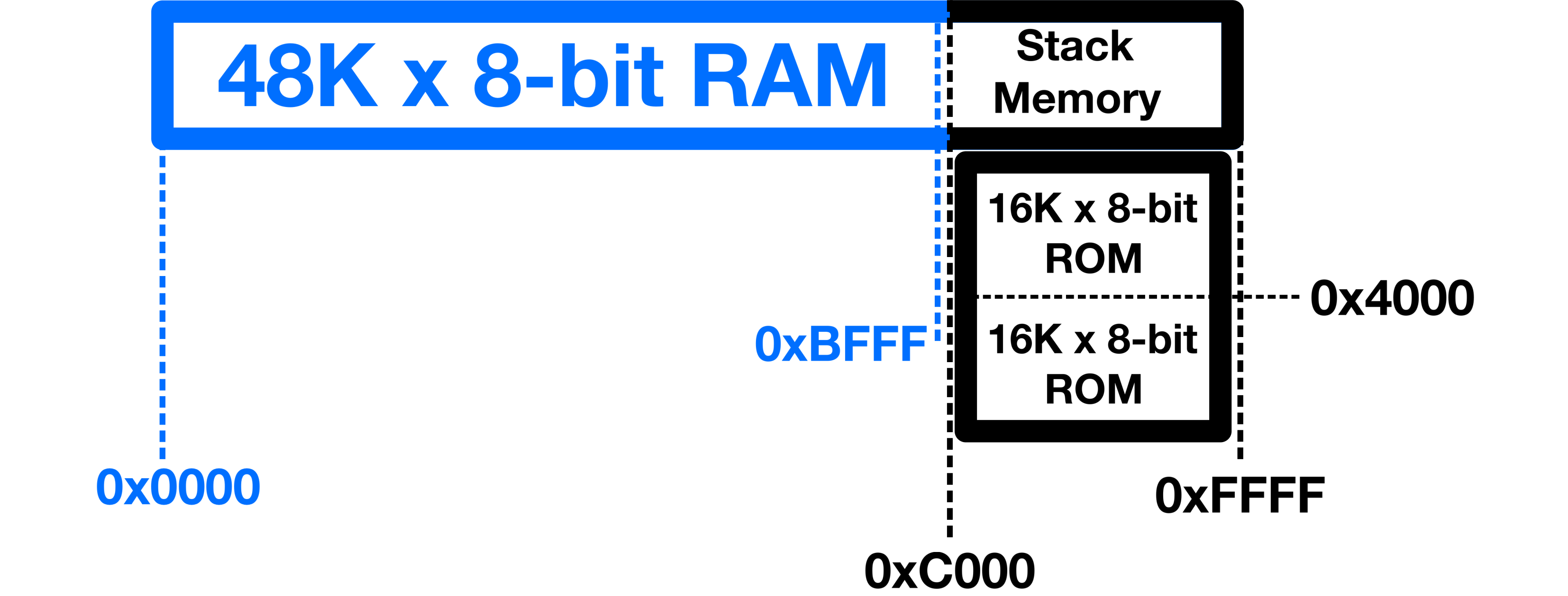
My RAM chip is a UM61512A 64K X 8 BIT HIGH SPEED CMOS SRAM, which is perfect for my use case, because it is cheap(About $15 for a set of 10 on Ebay), and very compact! The lower 48K of the memory is used for program memory, and the remaining/top 16K of memory is for either stack memory or a boot loader ROM.
The OS EEPROM is an X28C256, which is a 32K x 8-bit EEPROM. Since only a 16 KB window of the CPU’s address space is assigned to ROM at a time, only half of the EEPROM is visible in the memory map at once. To access the other half, I use a manual switch on the ROM’s most significant address input, which gives the same 16 KB ROM window access to either of the two 16 KB EEPROM banks.
Just like the SAP-1, my build can be set to either Programming or Run mode. When in programming mode, some DIP switches are used to manually point to memory addresses and enter data into RAM. An SPDT switch is used to switch between the two modes, and a push button is used to trigger the RAM’s write pin.
Below is a high level diagram to better illustrate the memory logic.
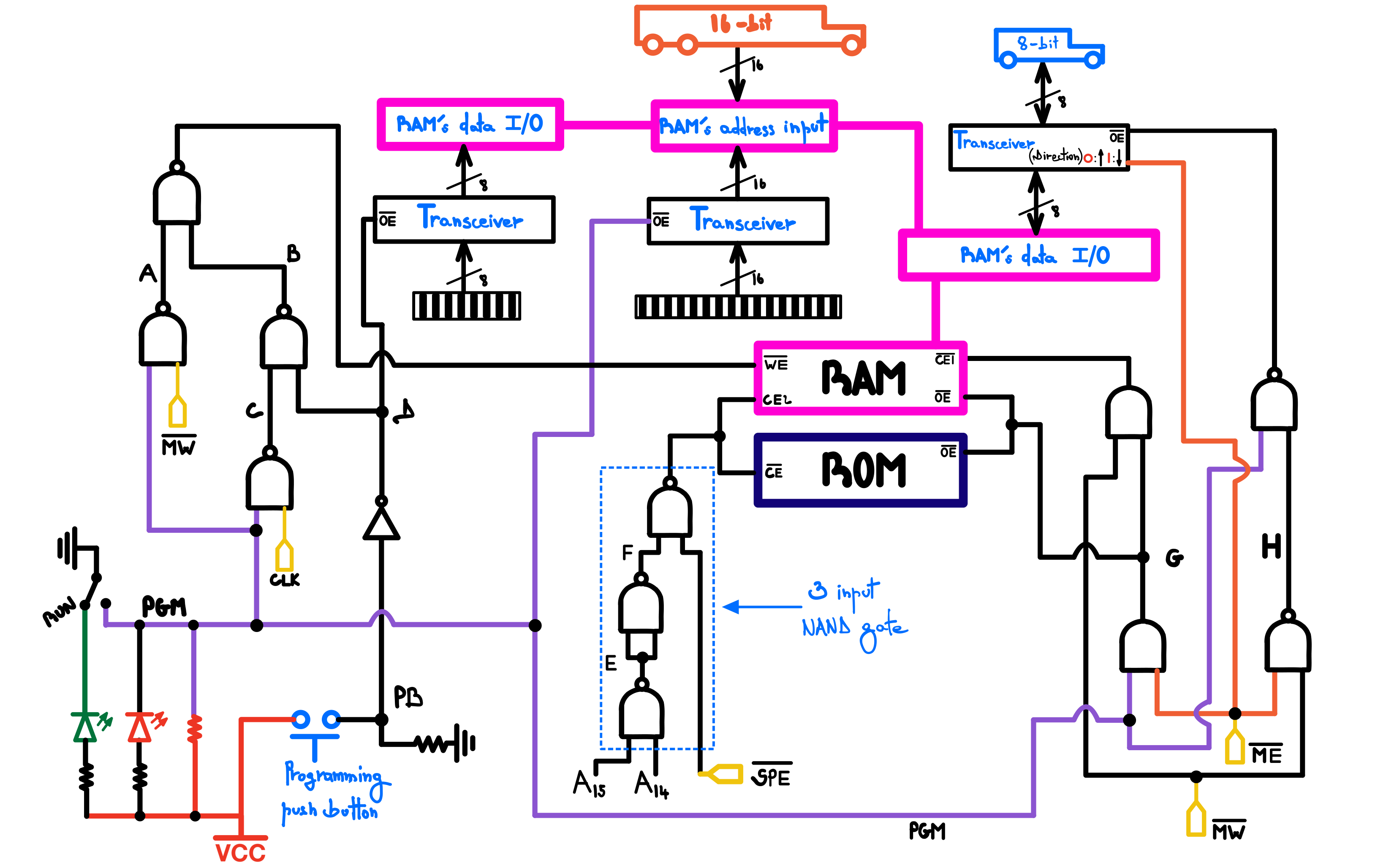
As mentioned before, addresses 0x0000 through 0xBFFF map to the lower 48 KB of SRAM. The upper 16 KB address range, from 0xC000 through 0xFFFF, can select either the bootloader ROM or the stack RAM path, depending on the state of ~SPE.
In binary:
0X0000        0000000000000000 }
                     |         }   RAM
                     ▼         }  memory
0XBFFF        1011111111111111 }

0XC000        1100000000000000 }
              ^^     |         } ROM & Stack
                     ▼         }   memory
0XFFFF        1111111111111111 }
The ROM/stack address range begins when the two most significant address bits, A15 and A14, are both HIGH. In other words, addresses from 0xC000 through 0xFFFF enter the upper 16 KB region. The bootloader ROM is selected from that region when ~SPE is inactive, or HIGH. A three-input NAND gate at the center of the diagram implements the selection logic.
The RAM chip conveniently has two chip-enable inputs: one active-low and one active-high.The output of the three-input NAND gate connects to the ROM’s active-low chip enable and the RAM’s active-high chip enable. As a result, the ROM chip remains inactive unless the CPU addresses the bootloader memory space.
The UM61512A RAM has all-in-one I/O data pins. With the appropriate control pins, it can either receive or output data through the same pins.
In Run Mode (PGM node is HIGH)
The RAM is controlled by the control logic, the I/O pins get routed to the data bus, and the address pins to the system bus:
Node D is HIGH, and C alternates between HIGH and LOW inversely to CLK, while B matches CLK. The RAM’s Write Enable (~WE) node is HIGH by default and goes LOW (at the rising edge of the clock) only when the Memory Write (~MW) control signal is active. Since both PGM and D are HIGH, the data and address input transceivers for the DIP switches stay locked (in high-impedance mode).
- When the Memory Enable(Enables memory content to data bus)(~ME) control line is active and ~MW is inactive, node H goes HIGH, G goes LOW, and the RAM’s data I/O transceiver directs data flow from the RAM’s I/O pins to the data bus.
- Inversely, when ~MW is active and ~ME is inactive, node H goes HIGH and the RAM’s data I/O’s transceiver directs data flow from the data bus to the RAM’s I/O pins.
- When neither ~MW nor ~ME is active, node H goes LOW, the RAM’s data I/O’s transceiver switches to high impedance mode, and the RAM chip gets disabled through ~CE1 as G and ~MW are HIGH.
~ME and ~MW being active at the same time is a forbidden state because you cannot read from and write to RAM simultaneously (at least not in my build).
Note: ~WE has priority over ~OE, provided the chip is enabled.
In Programming Mode (PGM node is LOW)
The RAM’s I/O pins get routed to the data DIP switches, and the address pins to the address DIP switches:
With PGM LOW, the address input transceiver connects the memory address DIP switch’s value to the RAM’s address input. The NAND gate on the far right of the diagram controls the I/O transceiver and outputs LOW, thus keeping the RAM from interacting with the data bus.
~MW and CLK now have no control over the state of ~WE because nodes A and C are always HIGH. Each time you press the programming push button, D goes LOW, which simultaneously activates ~WE and routes the data DIP switch value to the RAM’s data input pins.
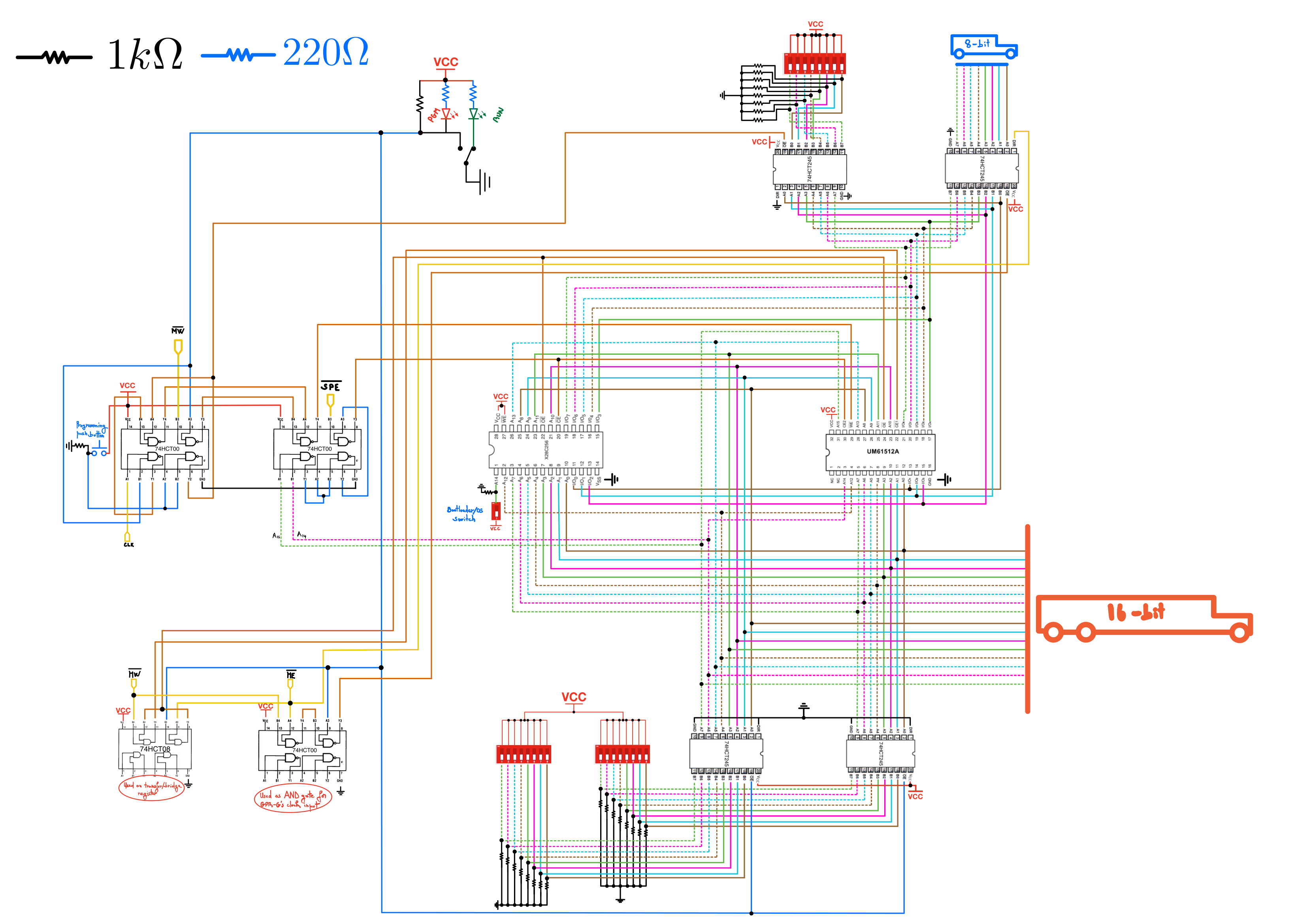
ICs
1x UM61512AK (Datasheet)
1x X28C256 32K x 8-bit EEPROM (Datasheet)
3x 8-bit DIP switch (Jameco).
8x 74HCT245, Octal Bus Transceivers With 3-State Outputs, (Digikey, Datasheet)
2x 74HCT574, 8-bit Octal D-Type Flip-Flop, 3-State (Digikey, Datasheet)
3x 74HCT00 Quadruple 2-Input Positive-Nand Gates (Digikey, Datasheet)
1x 74HCT08 QUAD 2-INPUT POSITIVE AND GATE (Jameco, Datasheet)