Bus & General Purpose Registers
Basics Primer
As mentioned in the overview, my build has an 8-bit data bus, and a 16-bit system/memory bus. “data bus” is somewhat of a misnomer given that all computer buses are involved in moving some form of data among various components and peripherals. In the context of this CPU, the data bus is used to transfer some control signals, memory locations(addresses) and I/O data, while the memory bus only deals with memory locations.
The use of a 16-bit address bus, which is explained in more details in the RAM post is an enhancement to the memory capacity without making the design overly complex. In simple terms, a 16-bit address bus allows the CPU to access a larger memory space compared to an 8-bit address bus. With 16 bits, the CPU can address up to 65,536 ($2^{16}$) individual memory locations, offering ample space to store and retrieve data and instructions.
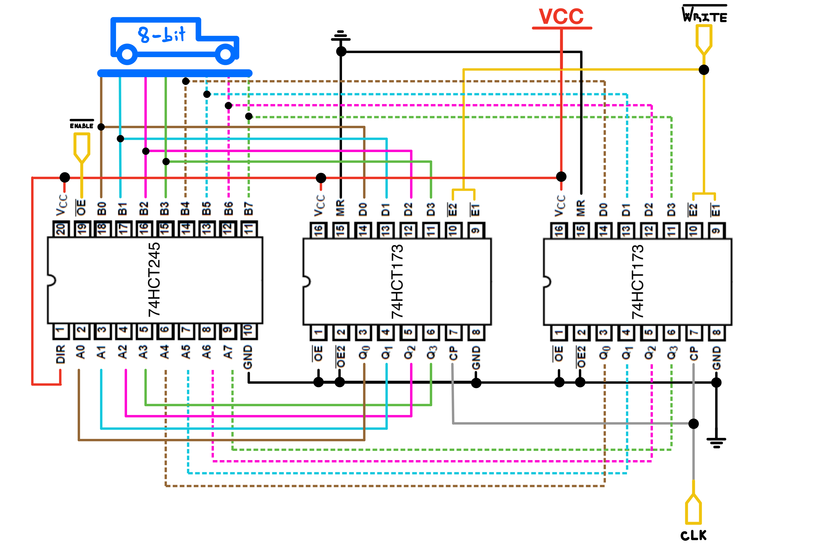
My build contains 5 general purpose registers (GPRs) A, B, C, D, and E; E being a partial GPR. All GPRs can read from and write to the 8-bit data bus. Four of them are dual 74HCT173(173) which I had assembled when initially building the SAP-1, and the last one is a 74HCT574(574).
Implementation
The 173 is a 4-bit register, therefore a pair is used with common control pins, to form a single 8-bit register. Although all of the GPRs are tri-sate, a 74HCT245 transceiver is used between the outputs of the 173s and the bus. This configuration allows for LEDs to display the content of the registers without causing interference on the bus. So essentially the bus transceivers serve as a final output-enable to the bus while the registers themselves are always outputting their content.
| Pin No | Pin Name | Description |
|---|---|---|
| 1 | DIR | Direction select(A to B, or B to A) |
| 2, 3, 4, 5, 6,7,8,9 | A1, A2, A3, A4, A5, A6, A7, A8 | Input/Output Pin 1, 2, 3, 4, 5, 6, 7, 8 |
| 10 | GND | Ground Pin |
| 11, 12, 13, 14, 15, 16, 17, 18 | B1, B2, B3, B4, B5, B6, B7, B8 | Output/Input Pin 1, 2, 3, 4, 5, 6, 7, 8 |
| 19 | ~E | Active Low Input Enable Pin |
| 20 | VCC | Chip Supply Voltage |
Table 1: 74HCT173 Pin Configuration
| Pin No | Pin Name | Description |
|---|---|---|
| 1, 2 | ~OE, ~OE2 | Active Low Output Enable Input 1 and 2 |
| 3, 4, 5, 6 | Q0, Q1, Q2, Q3 | Output Pin 0, 1, 2, 3 |
| 7 | CP | Clock Pulse Input |
| 8 | GND | Ground Pin |
| 9 | ~E1, ~E2 | Active Low Input Enable Pin 1, 2 |
| 11, 12, 13, 14 | D3, D4, D5, D6 | Data Input 3, 2, 1, 0 |
| 15 | MR | Master Reset Input |
| 16 | VCC | Chip Supply Voltage |
Table 2 74HCT245 Octal Bus Transceivers, Pin Configuration
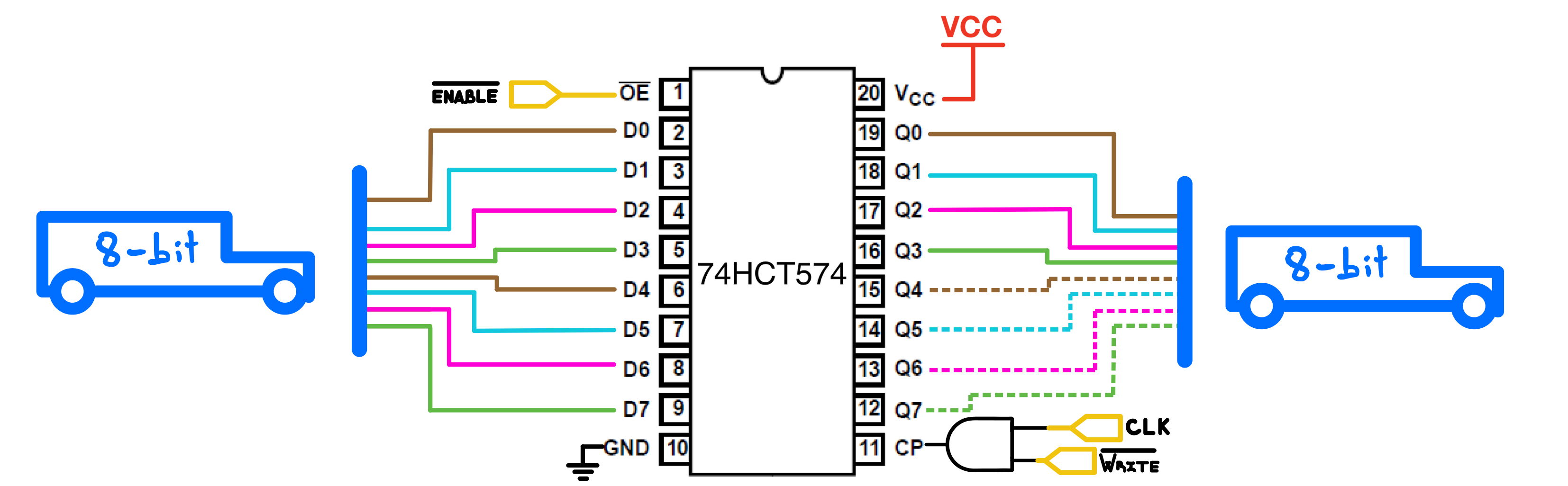
As can be seen, unlike the 74HCT173, the 74HCT574 does not have an enable pin. By default, the clock pin CP serves both as an enable and clock input pin, which means that at every rising clock edge, whatever appears on the data pins of the register would overwrite its content. This is obviously an undesired behavior. To solve this I simply AND the clock with the “write” control line for each 574, so that the register gets loaded/overwritten only when a “write” operation is asserted.
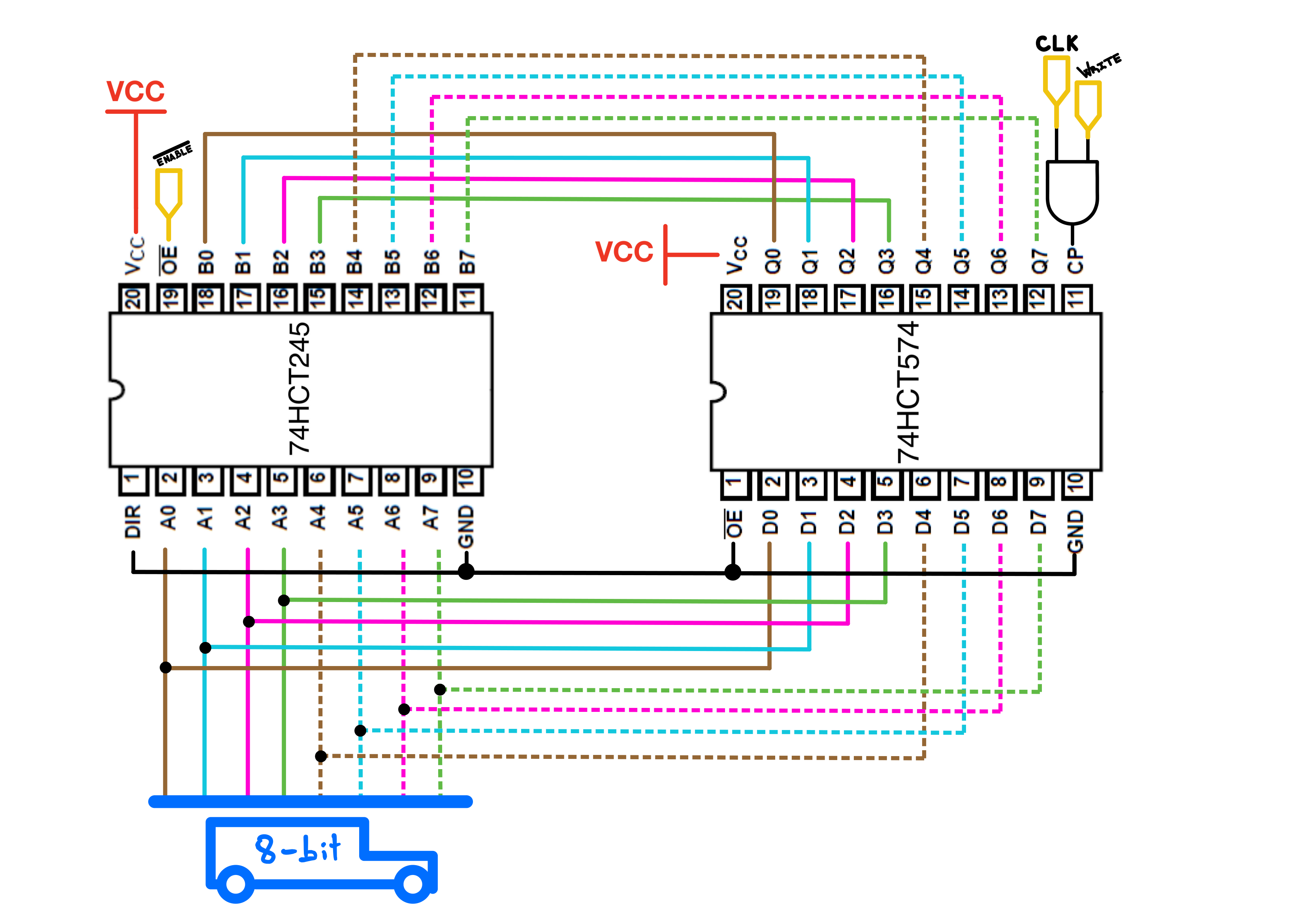
Unlike some other 8-bit register ICs with built-in gated enable, The 74HCT574 has a very clean pin layout: All inputs and outputs are aligned on opposite sides of the IC, which makes it very breadboard-friendly, just like the 74HCT173. Some of the 574s in my build are used without a transceiver due to space constraints on the breadboards.
| Pin No | Pin Name | Description |
|---|---|---|
| 1 | ~OE | Active Low Tri State Output Enable Pin |
| 2, 3, 4, 5, 6,7,8,9 | D0, D1, D2, D3, D4, D5, D6, D7 | Data Input Pin 1, 2, 3, 4, 5, 6, 7, 8 |
| 10 | GND | Ground Pin |
| 11 | CP | Clock Pulse Input |
| 12, 13, 14, 15, 16, 17, 18, 19 | O0, O1, O2, O3, O4, O5, O6, O7 | Tristate Output Pin 0, 1, 2, 3, 4, 5, 6, 7 |
| 19 | ~E | Active Low Input Enable Pin |
| 20 | VCC | Chip Supply Voltage |
Table 3: 74HCT574 8-bit Octal D-Type Flip-Flop Pin Configuration
ICs
8x 74HCT173, 4-Bit D-type Registers with tri-state Outputs, (Digikey, Datasheet)
1x 74HCT574, 8-bit Octal D-Type Flip-Flop, 3-State (Digikey, Datasheet)
4x 74HCT245, Octal Bus Transceivers With 3-State Outputs, (Digikey, Datasheet)
«««««««««« Previous Post: Permanent Clock
Next Post: ALU Primer »»»»»»»»»»
Updated: