EPROM Programmer
Basics Primer
I made a manual and an automatic EPROM programmer based off the ones developed by Ben Eater, and I implement the automatic programmer with an ELEGOO Nano Board. Both of my programmers are slightly different from the SAP-1’s because my ROM is wider and has a minor programming timing difference.
Note: I will refer to the Elegoo nano as the Arduino nano throughout this post. Elegoo is a company that legally offers a range of cost-effective copies (which work similarly to the originals) of Arduino boards, among other products.
As outlined in the overview post, I first built two versions/iterations of the SAP before making the current version. On the first one, I used the 11-address-line 28C16A 16K-Bit EEPROM from Ben Eater’s SAP-1 kit, and on the second I used a 15-address-line 28C256 256k-bit EEPROM. I had built the EPROM programmer for each version before completing the CPUs themselves. In my current build, I still use the 28C256, so this post focuses on the programmer I built for that EEPROM.
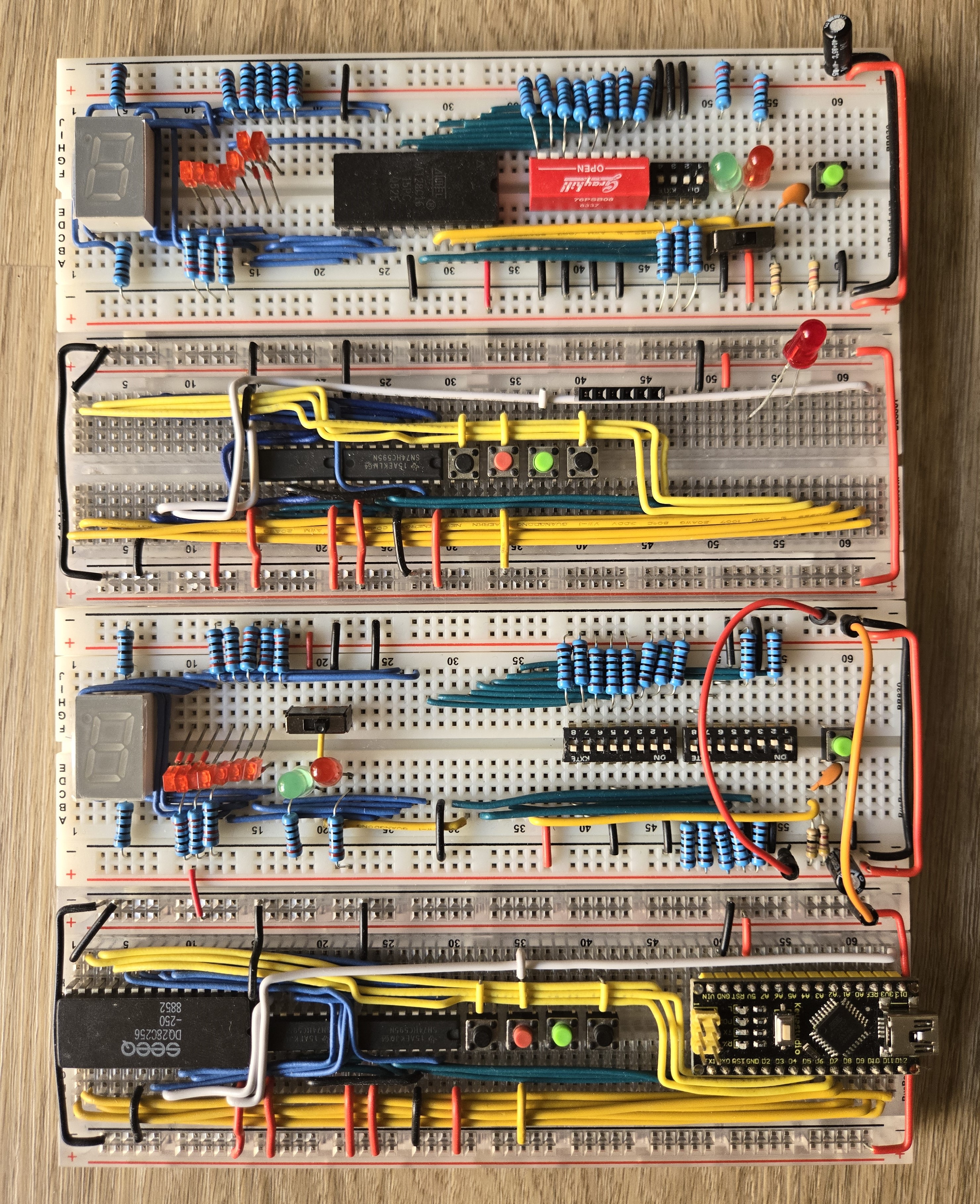
On the picture above, the top two breadboards contain the manual and Arduino based programmer for the SAP-1 EEPROM and the bottom two contain those of the 28C256, respectively. Do not mind the push buttons on the bottom breadboards, as they serve no practical purpose. In the current version of the CPU, the microcode ROMs are one of the biggest differences from Ben Eater’s original build. My control logic uses a different ROM organization, and some of the ROM chips I use have less convenient programming requirements, including EPROMs that need a 12V programming voltage. Since the Arduino Nano can only provide 5V without extra circuitry, I eventually moved to a dedicated GQ-4X4 USB programmer with a 16-bit EPROM adapter. I cover the microcode organization itself in the Microcode Generator post; this page focuses on the tools and workflow used to program the ROM chips.


Note: although the chips I use are M27C4002 EPROMs, the GQ programmer software repeatedly failed when I chose the M27C4002 device profile. In my setup, the TMS27PC240 profile worked instead. The two ROMs have the same pinout and compatible organization for this programming workflow, so I used the TMS27PC240 profile to write and verify the M27C4002 ROMs.
Another detail I should mention is how I erase the EPROMs. I don’t use a dedicated EPROM eraser. Instead, I use a small UV phone sanitizing box. The EPROMs have quartz windows, so the UV light can erase the stored charge over time.

The sanitizer runs on a short timer, so I usually run several cycles with the EPROM windows facing the UV lamp. After enough cycles, the chips erase fully and can be programmed again with the GQ-4X4 programmer. It’s not a professional EPROM-erasing setup, but it has worked reliably enough for my project.
The sanitizer was not designed specifically for EPROMs, the erase time is not precise; I verify the chips afterward in the programmer software before reusing them.
Implementation
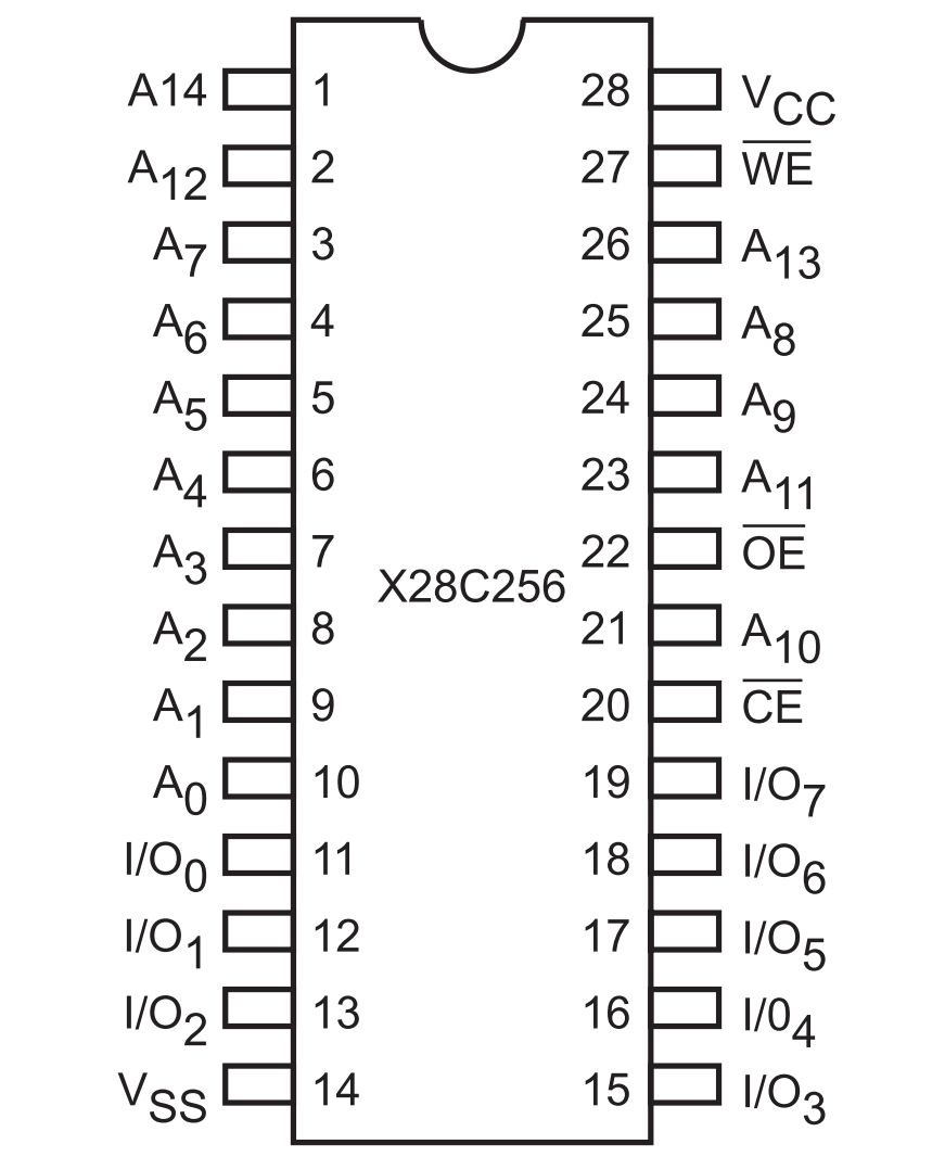
Below are the pinout and pin description of the X28C256:
On page 3 of the X28C256 Datasheet:
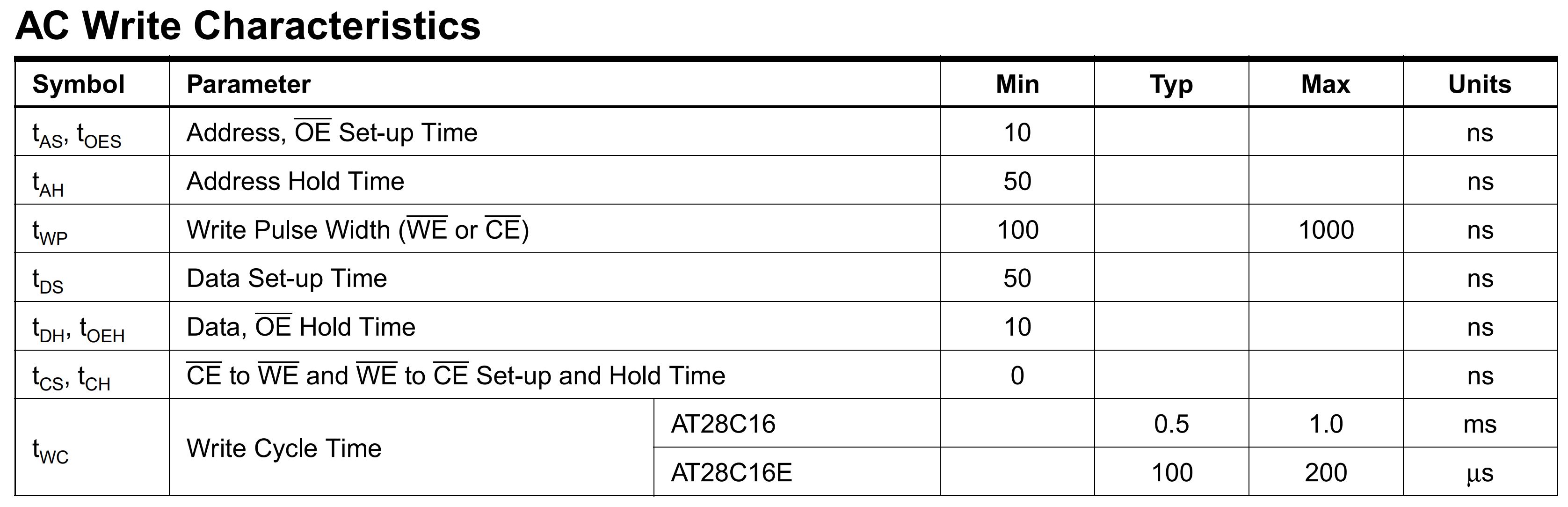
Write Write operations are initiated when both CE and WE are LOW and OE is HIGH. The X28C256 supports both a CE and WE controlled write cycle. That is, the address is latched by the falling edge of either CE or WE, whichever occurs last. Similarly, the data is latched internally by the rising edge of either CE or WE, whichever occurs first. A byte write operation, once initiated, will automatically continue to completion, typically within 5ms.
Similar to the EEPROM on the SAP-1, the state of either CE or WE can control the X28C256’s write cycle (I use WE).
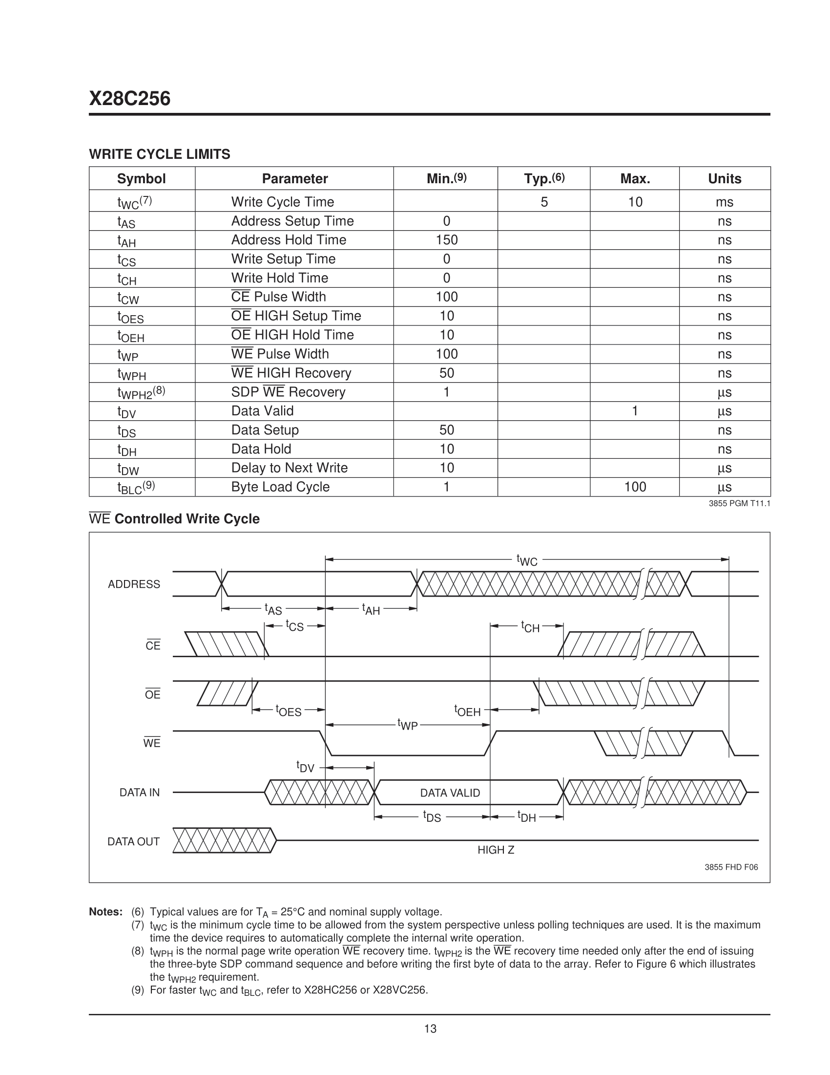
The figure above describes how to write to the X28C256 with WE as the control pin:
- Setup times are the time ranges a specific value must be held before taking effect in the write pulse width.
Hold times are the durations a value must be held after the edge at which it triggers.
For example: the address is latched by the falling edge of WE. tAH is the hold time of the address after WE’s falling edge
Similarly tOEH(OE high hold time) is OE’s hold time after WE’s rising edge.
In short:
- The write pulse must last at least 100 ns
- The address must be 1- set before the falling edge of WE, 2- held for 150ns at least.
- The data must be 1- set before the rising edge of WE, for at least 50ns; 2- held for at least 10ns.
The manual circuit
Now let’s implement Ben Eater’s fully manual EEPROM programmer. The only difference is that my programmer supports more address lines. The circuit lets you enter values to specific addresses of the EEPROM IC under its programming time constraints.
Side Notes Related to Ben Eater’s EEPROM
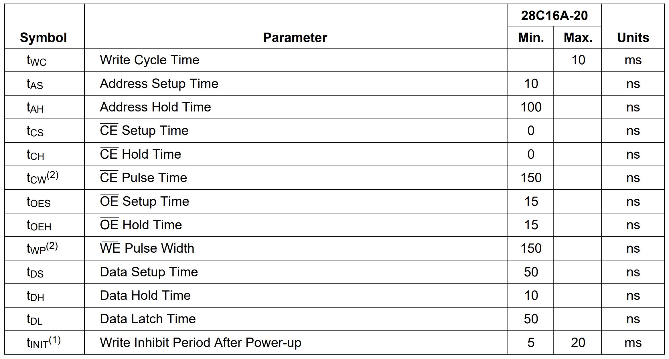
Before making the circuit for the X28C256, I experimented with the 28C16A from Ben’s build. I noticed that depending on the manufacturer of the 28C16, the chip may have a different maximum write pulse width, or no listed maximum write pulse width at all. For example, Figure 8 shows the 28C16A write-cycle limits from Microchip Arizona Semiconductors, Figure 9 is from Catalyst, and Figure 10 is from Atmel.
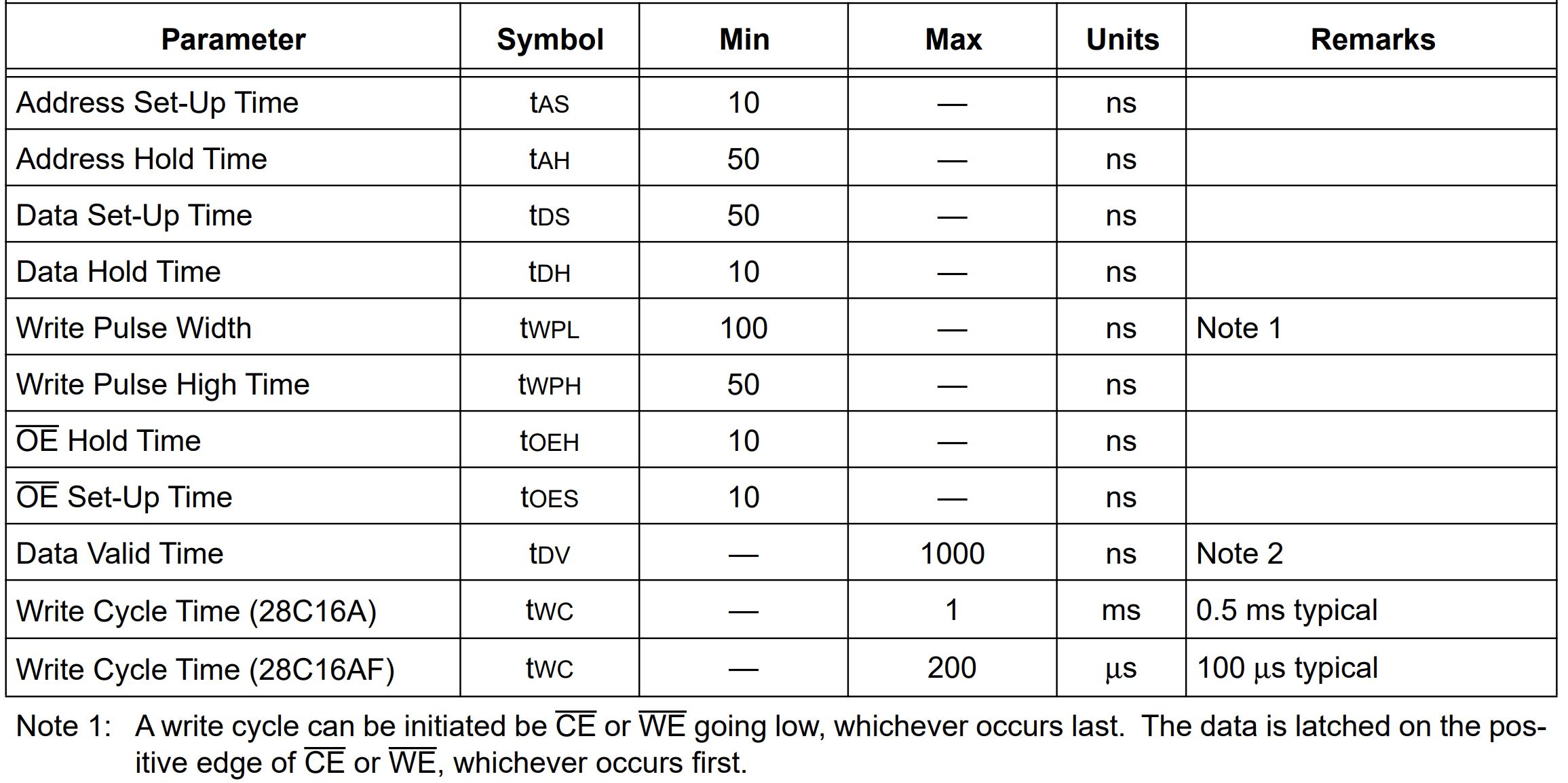
Most of the time, the minimum write pulse time for the 28C16 EEPROM is around and no longer than 150ns. A push button will almost always exceed that time, unless your finger can move at the speed of light.
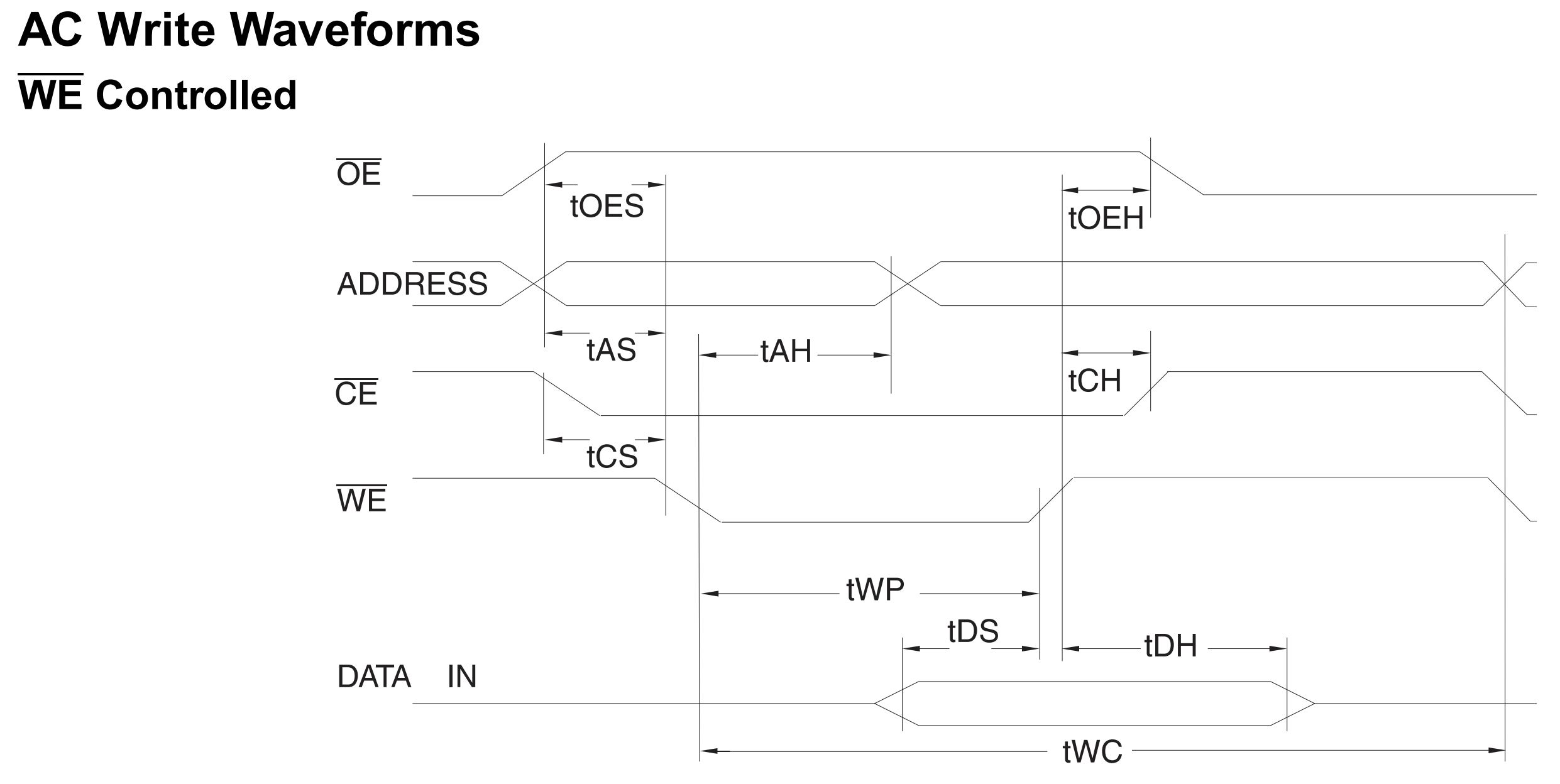
Figure 11 shows the 28C16’s write waveforms based on WE.
No matter which type of 28C16 EEPROM you end up using, they are always going to have about the same minimum write pulse time. The most important distinction would be the maximum pulse time. Since at least one 28C16 has a maximum $tWP$ of 1000 ns, it is useful to have an RC push-button circuit that keeps WE LOW for a duration between 150 ns and 1000 ns. This push button circuit works on most 28C16 EEPROMs whether they have a maximum write pulse time or not. Since it is just an RC circuit, you can easily tune its time constant to meet the other chips’ write-time requirements.
NB: Although I have not yet seen a 28C256 with a $tWP_{max}$, I still implemented the push button circuit on my manual X28C256 programmer.
Description of the push button circuit.
Since WE is an inverted input, the write pulse should start after WE falls from VCC to ground, and end after WE rises back to VCC. To make sure WE stays low only within the $[tWP_{min}, tWP_{max}]$ time window, Ben Eater pairs a $0.01uF$ capacitor in series with a $680Ohm$ resistor to create a time constant of approximately $680ns$. That falls well within his range of $150ns$ to $1000ns$. I did not have these exact values at hand when I built my programmers, so I used a $47Ohm$ resistor and a $0.01u$F capacitor to produce a time constant of approximately $470ns$, which again falls between the $150ns$ to $1000ns$ time range. Below, is a Falstad simulation of the circuit.
Note that the values picked for this simulation were chosen because the simulator’s oscilloscope cannot properly simulate shorter pulses: The resistor and capacitor values on my physical circuit are 47Ω and 0.01uF respectively.
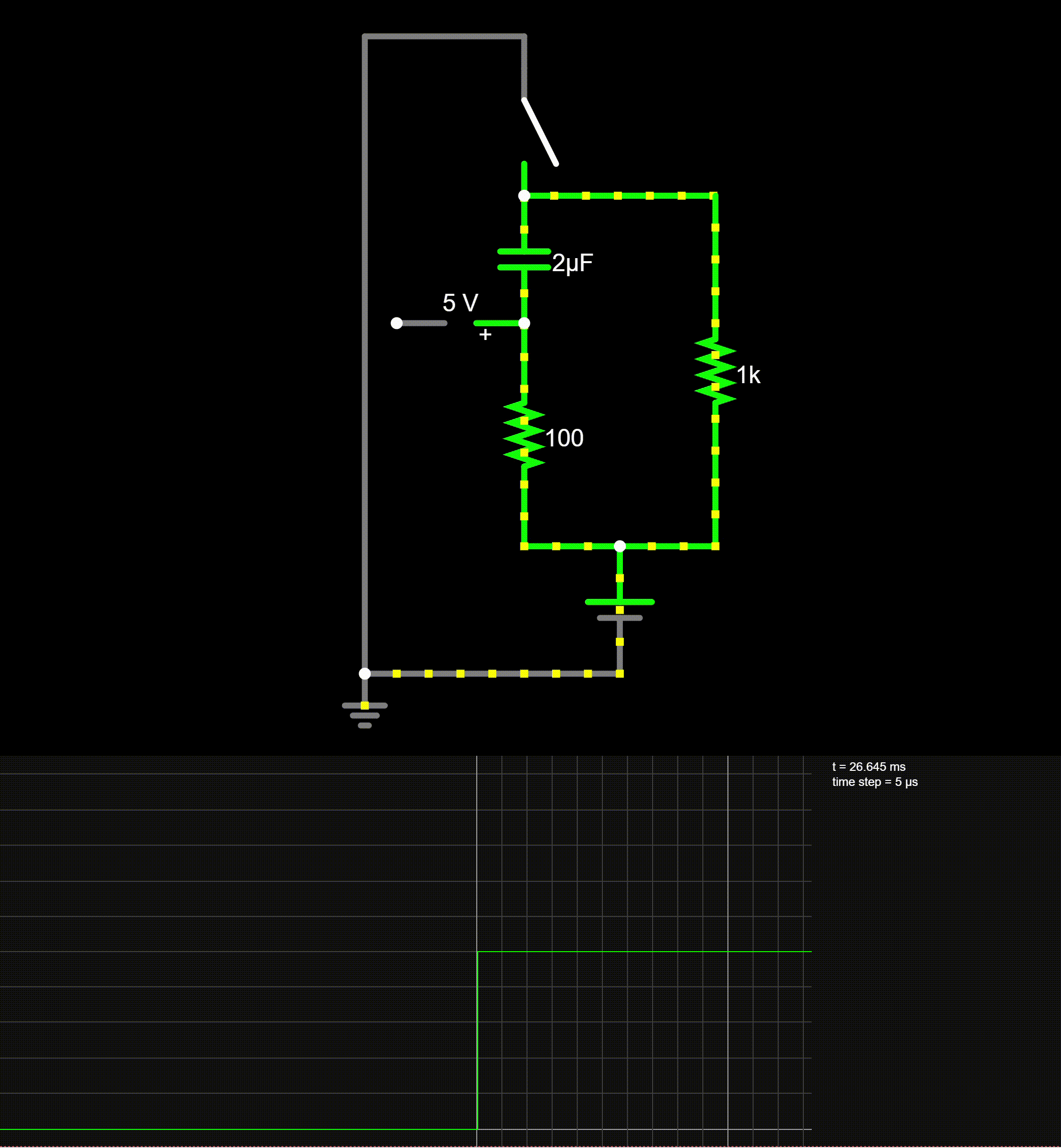
The oscilloscope is showing the node between the capacitor and the 100 Ohm resistor. Let’s call it node A. Assuming stable initial conditions (the push button has never been pressed):
- When the push button is open, the voltage(potential to be correct) at node A is the same as the battery’s positive terminal, because there is no current flow, therefore no voltage drop.
- Right at the instant when the switch is closed, the voltage at node A “falls” to zero because the net charge on each of the two plates of the capacitor is equal(The plates are at equipotential).
- After closing the switch, the capacitor takes roughly $0.2ms$ to charge up. In other words, it takes roughly $0.2ms$ for node A to reach $5V$.
- After opening the switch, the capacitor discharges(In conventional current flow) through the $1kΩ$ resistor.
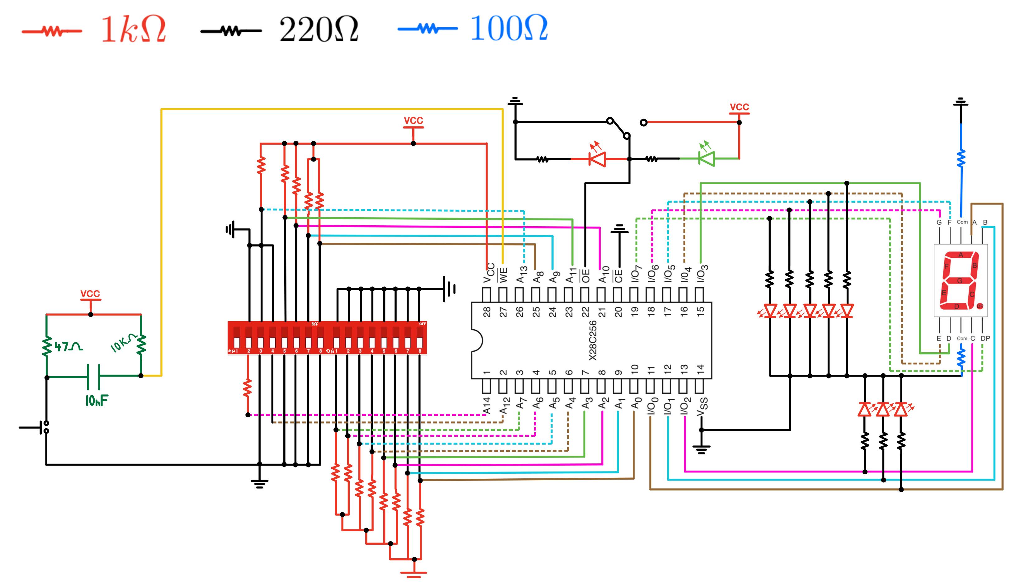
Below is a schematic of the manual programmer, with a “witness” seven segment display on the right.
The Arduino EPROM programmer
If you do not have it already, follow this link to download Arduino IDE.
The Arduino Integrated Development Environment (IDE) is software that lets users write and upload code to the microcontroller on the Arduino board. It uses a variant of C++ (with additional special methods and functions) and provides a simple and intuitive interface to write, test, and debug code.
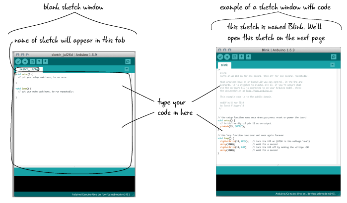
You can follow the link to the image above for an extensive guide on how to use an Arduino board. After installing Arduino IDE, plug the Arduino nano to your computer and follow these steps:
1- Launch Arduino IDE.
2- Open a test sketch(Sketches are just programs): Files » Examples » 01.Basics » Blink. A new windows should open, with the “blink” sketch pre-written.
- On the new window:
- Select your board: Tools » Board » Arduino AVR Boards » Arduino Nano
- Select your Serial port: Tools Serial Port » pick the port on which the Arduino is connect. You can check which port it is in your device manager; or simply disconnect your board and re-check the port list to find out which port has disappeared.
- Upload the sketch.
- If everything is setup correctly you should see an LED blinking on your Arduino board.
Note:
- A sketch is just a Program/code.
- The void setup() and void loop() functions are mandatory. Omitting any of them in a sketch will result in a compilation error.
- The reset push button on the Arduino does not erase its flash memory/ROM, but just its RAM. It simply restarts the Arduino. Once a code is uploaded onto the Board it stays on its flash memory and can be used without the board having to be connect to a computer.
For Linux Users:
From GitHub: “Some Linux distros have a pre-installed application named BRLTTY that interfaces the terminal with braille displays. These displays use a serial port for communication with the computer. Unfortunately, BRLTTY assumes that the port from any general purpose USB to serial adapter is a braille display and takes over the ports. If the port is actually of an Arduino board, this causes the port to not appear in the Arduino IDE ports list.”
This kept me from interfacing with my Arduino; so if you do not need BRLTTY, uninstall it with:
sudo apt-get remove --auto-remove brltty
The “auto-remove” option is to remove packages that were automatically installed to satisfy dependencies for BRLTTY.
You might now see the board’s port in Arduino IDE and still get the following error:
avrdude: ser_open(): can't open device "/dev/ttyUSB0": Permission denied
This is probably because you are not a member of the dialout group. Members of this group have full access to the serial port.
To check whether you are a member of dialout or not, open a terminal window and enter:
groups
If dialout is not among the groups listed, enter the following in your terminal:
sudo adduser your_username dialout
And reboot your computer.
After following these steps you should be added to dialout and interface with your Arduino board.
I/O Pin Limitations
As a reminder, the X28C256 has 28 pins in total, and the writing process requires interactions with 25 of them(All pins except VCC, CE, and GND). The Arduino Nano however only has 14 digital I/O pins(And only 12 remain controllable when using the USB port). The analog pins can also be used as digital pins, but on the Arduino Nano, A6 and A7 are analog-input-only. Even after using the available analog pins as digital pins, the Nano still does not provide enough I/O pins to directly control all of the EEPROM address, data, and control pins.
A solution (covered by Ben Eater) to this is to use shift registers, which commonly “translate” parallel data to serial data, or vice versa. It is common practice to implement them to “expand” the number of I/O pins on a microcontroller.
Shift Registers
This programmer operates with a Serial-In-Parallel-Out (SIPO) shift register, which, as its name suggests, takes a serial input (data sent bit by bit) and produces a parallel output (data sent in batch).
Shift registers are often made using cascaded D flip-flops with a synchronous clock. I made a simple Falstad schematic of a 4-bit shift register:
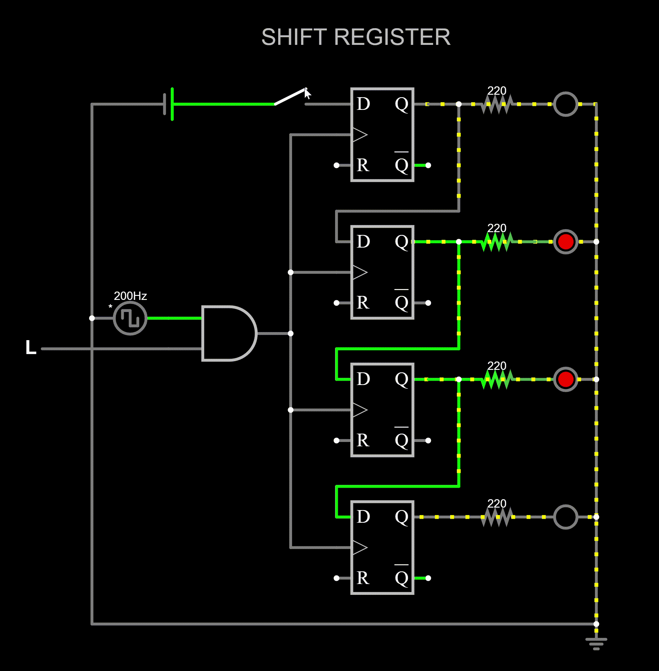
The AND gate on the left serves as a clock enable. At the rising edge of the clock, whatever value is present at the input of the topmost flip-flop propagates through the input of the next flip-flop, which in turn propagates its output to the following flip-flop, and so on. To program the EEPROM, you must set the address pins to select the location where data writes, and the data pins to define what writes. Because the Arduino Nano lacks enough pins to directly interface with all the ROM pins, a shift register serializes the control signals. This means you can send the address and data information one bit at a time, rather than all at once.
To program the EEPROM, you need a register that can “hold” arbitrary output states, among other things. The 74HC595 8-Bit Shift Register is an excellent candidate for this.
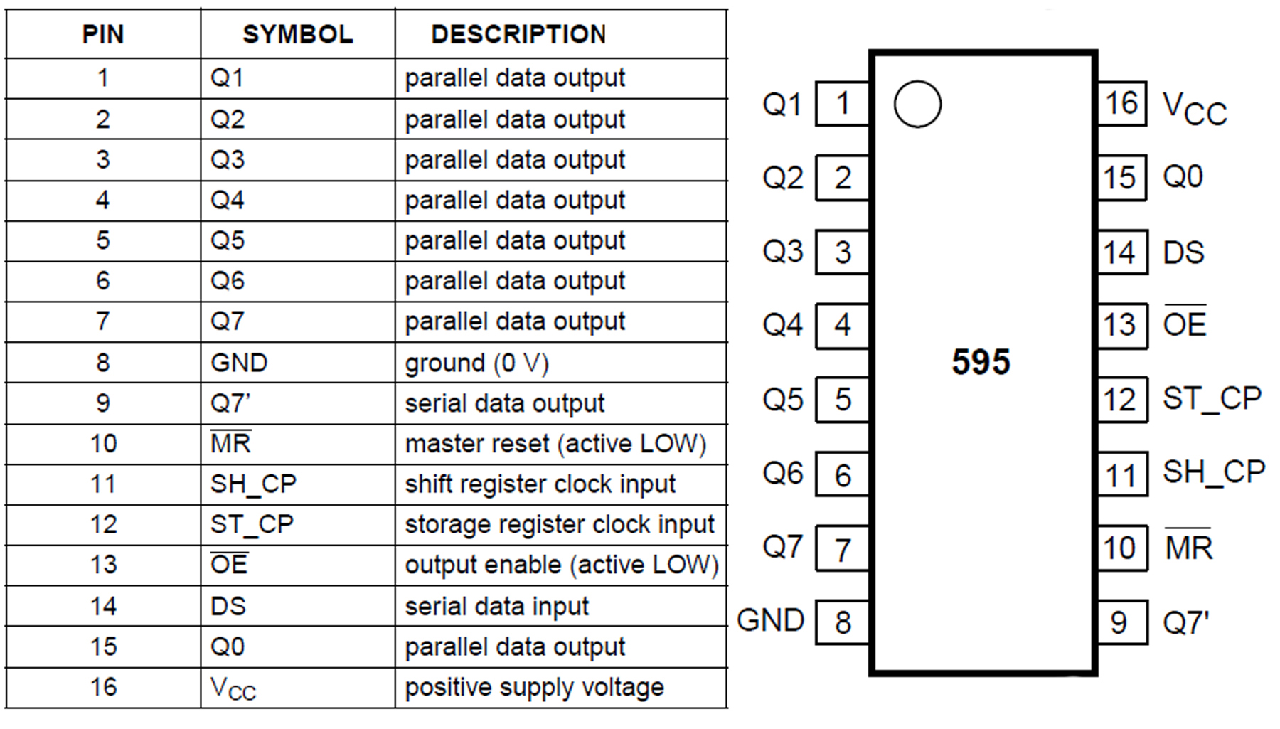
Note that pins 11 and 12 in Figure 17 refer to two different registers. In fact as can be seen from the figure below, the 74HC595 has two sets of flip-flops.
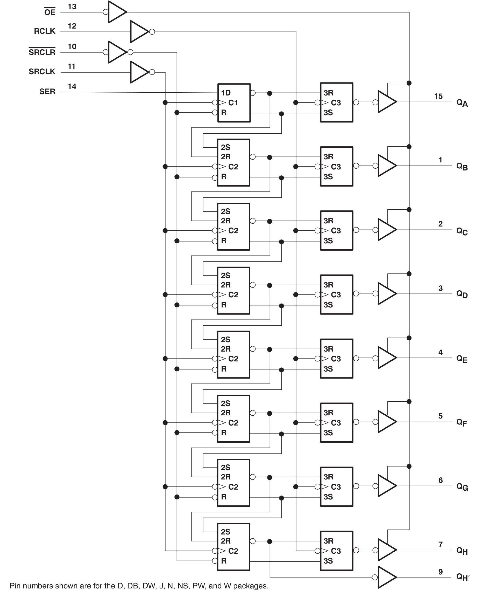
The left-most column of flip-flops makes up the actual shift register, and the rightmost column is the storage register. The storage register, which clocks independently of the shift register, buffers the output data. This holds the output data as-is while the system loads the next serial input data. Additionally, the storage register has a tri-state parallel output to provide even more flexibility.
A 16-bit shift register is formed by connecting pin 9 (Serial Data Output 7) from one 74HCT595 to pin 14 (Serial Data Input) of another. The Serial Data Input pin of the first register then serves as the input for the 16-bit register. Loosely speaking this connection follows the same cascading logic as in figure 16. And obviously, the Serial and Data clock input of both registers must be joined.
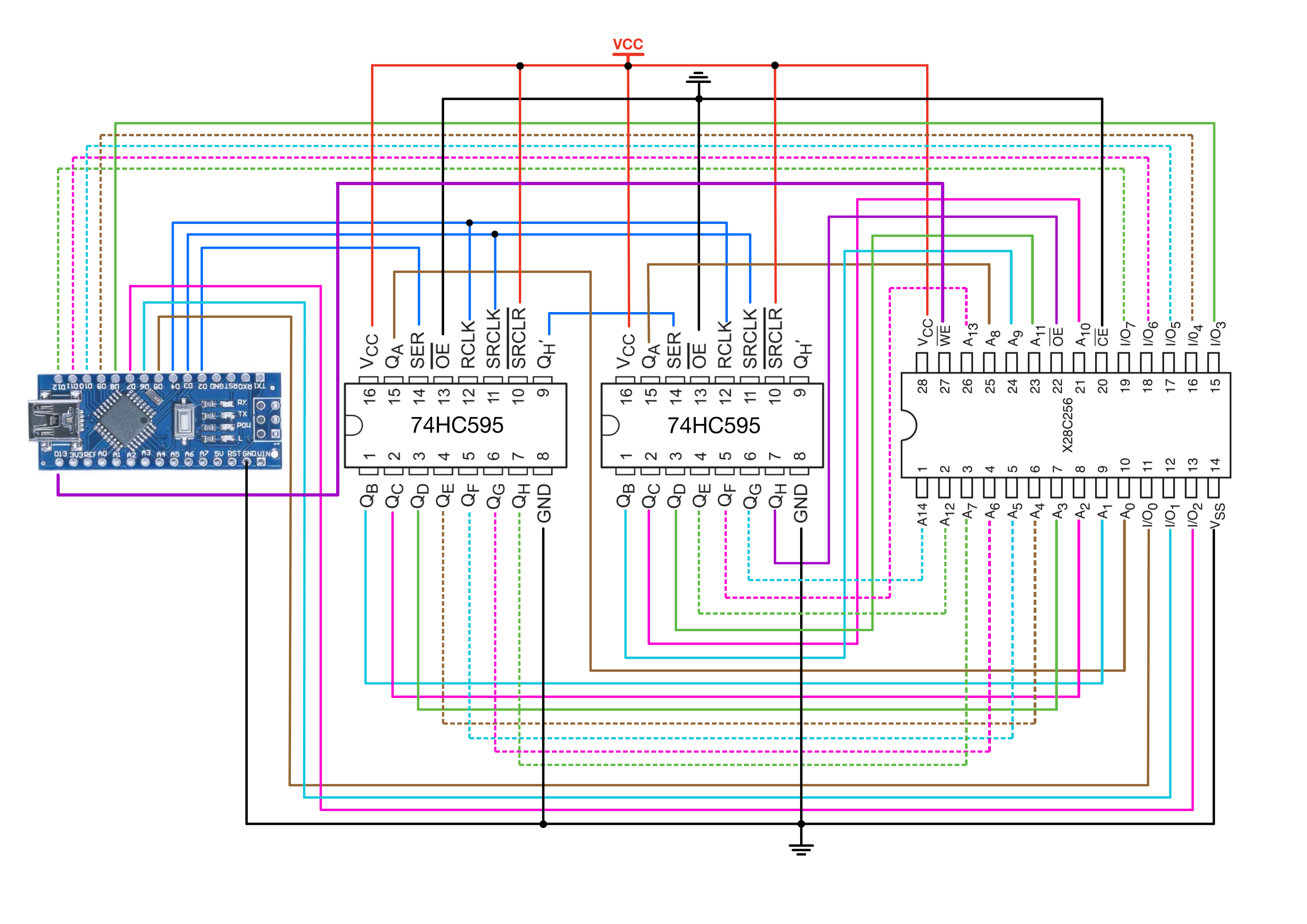
Three of the outputs from the Arduino’s few available I/O pins are tied to 16-bit shift register’s control pins. The Arduino can then send data in a serial format to the shift register. Each bit is clocked into the shift register sequentially, and once the complete set of data is clocked in, the shift register can then present all the data at its outputs simultaneously in parallel. This parallel data is then used to set the state of the address and data lines on the ROM.
Programmer Code
Timing Constraints
In the Arduino variant of C++, there is no built in function to provide a delay of less than one micro-second. Ben Eater uses a 1 micro-second delay to program his EEPROM, which works perfectly. However, if you are curious about how to get more accurate delays within the allowed setup time range; it is achievable with a simple Assembly language macro. In C++, Assembly declarations give the ability to embed Assembly language source code within a program; A NOP instruction takes one clock cycle. The ATmega328 chip used in the Arduino nano has a 16MHz clock speed(16 Million cycles every second) which means that a NOP would take (1/16MHz) ==> 62.5ns.
/// Defining macros///
#define NOP __asm__ __volatile__ ("nop\n\t""nop\n\t""nop\n\t""nop\n\t")
NOP; // Delay of 250ns on a 16MHz AtMega
The NOP macro executes four NOPs back-to-back, resulting in a 250ns delay, which is within the EEPROM’s write time range[100ns, 1000ns].
// Pin definitions for interfacing with shift registers and EEPROM
#define data_pin 2
#define clk_pin 3
#define content_register_pin 4

#define EEPROM_D0 5  // LSB of EEPROM data pins
#define EEPROM_D7 12 // MSB of EEPROM data pins
#define WRITE_EN 13  // EEPROM Write Enable pin

// Default value for padding
const byte DEFAULT_PADDING_VALUE = 0xFF;
The padding value is written when erasing memory locations.
The setAddress function sends the address to the EEPROM with an option to enable or disable the output.
shiftout() sequentially raises CLK and shifts a byte one bit at a time. Syntax: shiftOut(dataPin, clockPin, bitOrder, value)
bitOrder simply defines in which order data must be shifted out. bitOrder: MSBFIRST or LSBFIRST.
void setAddress(int address, bool outputEnable) {
  // Shifting out the high byte of the address with the output enable signal
  shiftOut(data_pin, clk_pin, MSBFIRST, (address >> 8) | (outputEnable ? 0x00 : 0x80));
  // Shifting out the low byte of the address
  shiftOut(data_pin, clk_pin, MSBFIRST, address);

  // Triggering the storage register to latch the data
  digitalWrite(content_register_pin, LOW);
  digitalWrite(content_register_pin, HIGH);
  digitalWrite(content_register_pin, LOW);
}
As a reminder, the output enable pin of the EEPROM is connected to the very last pin of the second 74HC595(Upper byte). Doing a bitwise OR of the address with 0x80 (00000000_10000000) in binary) determines whether the output enable gets set or not.
For example x80 OR x05:
00000000_10000000 (x80)
00000000_00000101 (x05)
= 00000000_10000101
This triggers the ~OE bit without changing the value of the address.
The read_byte() function reads data from the EEPROM one byte at a time, and sets proper address setting before data retrieval.
byte read_byte(int address) {
  // Setting EEPROM data pins as inputs
  for (int pin = EEPROM_D0; pin <= EEPROM_D7; pin += 1) {
    pinMode(pin, INPUT);
  }
  // Setting EEPROM address and output enable to begin the read operation
  setAddress(address, /*outputEnable*/ true);

  // Reading the data byte, bit by bit from the EEPROM
  byte data = 0;
  for (int pin = EEPROM_D7; pin >= EEPROM_D0; pin -= 1) {
    data = (data << 1) + digitalRead(pin); // Assembling the byte from individual bits
  }
  return data;
}
The write_byte function writes a byte of data to a specific address in the EEPROM. It sets the necessary pins as outputs, sends the address, and then writes the data. The NOP macro is used here to provide the necessary timing delay for the write cycle.
void write_byte(int address, byte data) {
  // Setting address and unsets output enable before the write operation
  setAddress(address, false);

  // Configuring EEPROM data pins as outputs
  for (int pin = EEPROM_D0; pin <= EEPROM_D7; pin += 1) {
    pinMode(pin, OUTPUT);
  }

  // Writing the byte to the EEPROM, bit by bit
  for (int pin = EEPROM_D0; pin <= EEPROM_D7; pin += 1) {
    digitalWrite(pin, data & 1); // Writing LSB of the data
    data = data >> 1;           // Shifting data to get the next bit to write
  }
  digitalWrite(WRITE_EN, LOW);  // Enabling write operation
  NOP;                          // Short delay of 250ns
  digitalWrite(WRITE_EN, HIGH); // Disabling write operation
  delay(10);                    // It gives enough time for data to latch before the next cycle begins.
}
read_ROM reads and formats the EEPROM contents into a human-readable form. The contents are displayed in the Serial Monitor accessible via Tools > Serial Monitor or (Ctrl+Shift+M). “address_offset” allows reading and printing from a specific address in the EEPROM.
void read_ROM(unsigned int address_offset = 0) {
  // Reading and printing EEPROM contents by iterating over each data byte
  Serial.println("Reading EEPROM");

  for (int base = address_offset; base <= (255 + address_offset); base += 16) {
    byte data[16]; // Buffer to hold the data read

    // Reading a block of data
    for (int offset = 0; offset <= 15; offset += 1) {
      data[offset] = read_byte(base + offset);
    }

    // Formatting the data into a string for output
    char buf[80];
    sprintf(buf, "%03x:  %02x %02x %02x %02x %02x %02x %02x %02x
    %02x %02x %02x %02x %02x %02x %02x %02x",
            base, data[0], data[1], data[2], data[3], data[4], data[5], data[6], data[7],
            data[8], data[9], data[10], data[11], data[12], data[13], data[14], data[15]);

    Serial.println(buf); // Sending the formatted data to the serial monitor
  }
}
erase_ROM erases the ROM starting from a specified address offset.
void erase_ROM(unsigned int address_offset = 0) {
  // EEPROM erase sequence
  Serial.print("Erasing EEPROM");
  for (int address = address_offset; address <= 32767; address++) {
    write_byte(address, DEFAULT_PADDING_VALUE); // Writing all bits to 1 (erased state)

    // Progress indication
    if (address % 3200 == 0) {
      Serial.print("."); // Print a dot for every 3200 addresses erased
    }
  }
  Serial.println(" done");
}
Finally, write_to_ROM writes an array of data to the EEPROM starting from a specified address offset.
void write_to_ROM(byte data[], size_t size, unsigned int address_offset = 0) {
  // EEPROM programming sequence
  Serial.print("Programming EEPROM");
  for (size_t address = address_offset; address < size + address_offset; address++) {
    write_byte(address, data[address - address_offset]); // Writing predefined data to EEPROM

    // Progress indication
    if (address % 2 == 0) {
      Serial.print("."); // Print a dot for every 2 addresses programmed
    }
  }
  Serial.println(" done");
}
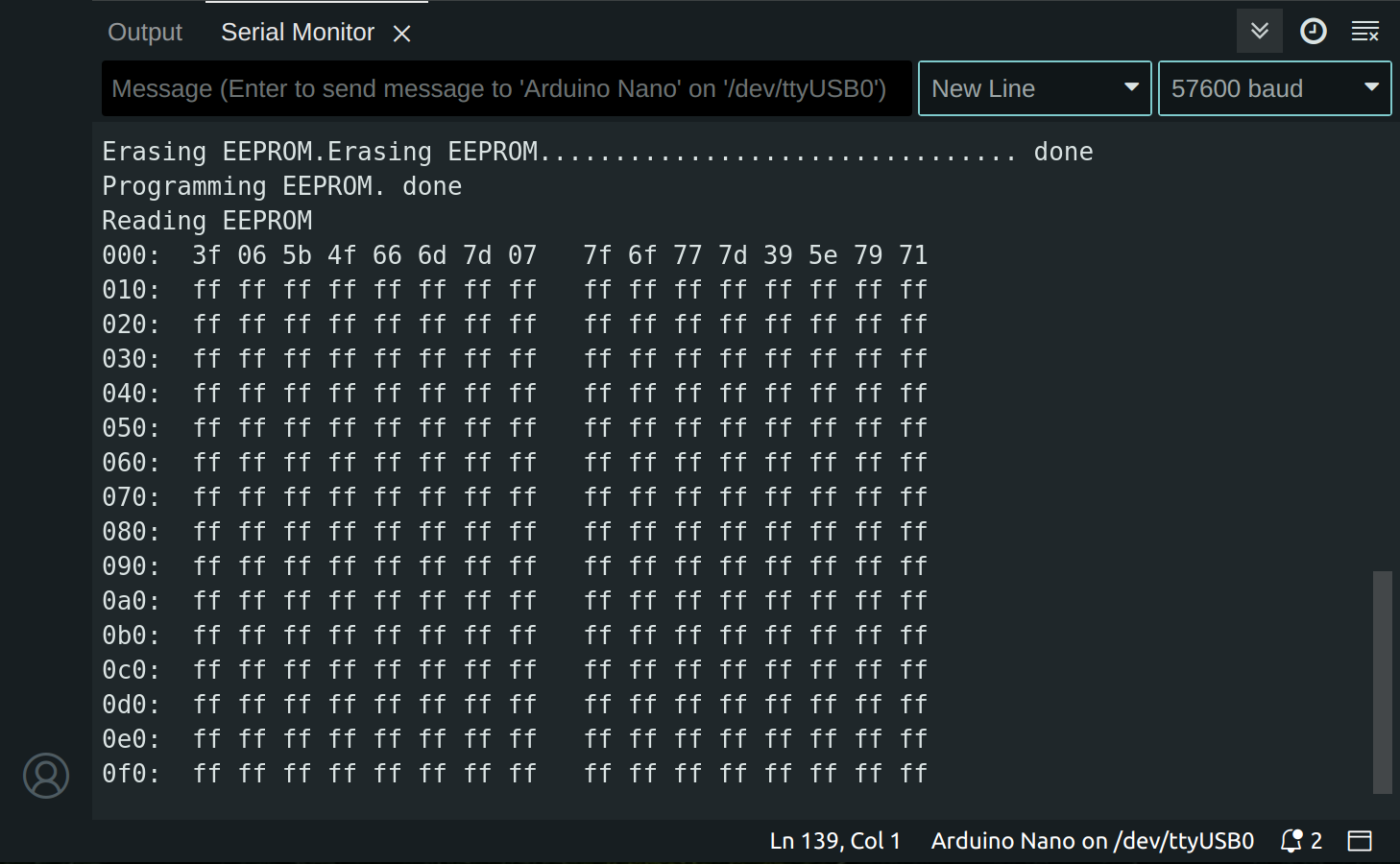
To triple check that the code is working, I just test it by uploading erase_ROM() and I wait for about 5 seconds; which should be more than enough to erase the first few addresses. Next I write “0” to “15” following my manual programmer’s BCD encoding on the first 16 addresses and I check the ROM’s content on the manual switch.
Note: When using the Serial Monitor, make sure to match the baud rate from the code to one of the ones available in the monitor. The baud rate is an important parameter in setting up serial communications because it determines the speed at which data is sent and read over a serial line. If the baud rates in a serial communication do not match, the receiving device may interpret the incoming bits incorrectly.
// Array to hold 7-segment display encoding for hexadecimal digits
byte data[] = { 0x3f, 0x06, 0x5b, 0x4f, 0x66, 0x6d, 0x7d, 0x07,
0x7f, 0x6f, 0x77, 0x7d, 0x39, 0x5e, 0x79, 0x71 };

void setup() {
  // Setting up the pins for communication with shift registers and EEPROM
  pinMode(data_pin, OUTPUT);
  pinMode(clk_pin, OUTPUT);
  pinMode(content_register_pin, OUTPUT);
  digitalWrite(WRITE_EN, HIGH); // Makes sure EEPROM is not writable on setup
  pinMode(WRITE_EN, OUTPUT);

  // Initializing serial communication with the specified baud rate
  Serial.begin(57600);

// Find the size of the data array
size_t dataSize = sizeof(data) / sizeof(data[0]);

// Write/Read/Erase either first or second half of ROM.
//unsigned int offset = 16384; // Second half

erase_ROM();
write_to_ROM(data, dataSize);
read_ROM();

}

void loop() {
}
Parts and Tools
1x 74HC595 8-bit shift register with 3-state output register (Digikey, Datasheet)
1x ELEGOO Nano Board CH340/ATmega328P, Arduino Nano-compatible, without USB cable (Amazon)
1x GQ-4X4 USB universal programmer with ADP-054 16-bit EPROM adapter (Amazon, MCUmall)