Program Counter & Stack Pointer
Basics Primer
The Program Counter(PC), also known as Instruction Address Register, the Instruction Counter, or the Instruction Pointer, is a special-purpose register in a CPU that contains the address of the instruction being executed. As each instruction gets fetched, the Program Counter increments its stored value by 1.
In addition to the PC, another essential component in a CPU is the Stack Pointer(SP). The Stack Pointer is a special-purpose register that primarily tracks the top of the stack in memory. In many CPU architectures, the stack is a region of memory that stores temporary data such as function parameters, return addresses, and local variables. The Stack Pointer increments or decrements its value depending on whether data is pushed to or popped from the stack, respectively.
J-K Flip Flop
The SR flip-flop/latch has an invalid input state when S = R = 1.
The JK flip-flop eliminates this issue by introducing a new input state which triggers a toggle action when J = K = 1.
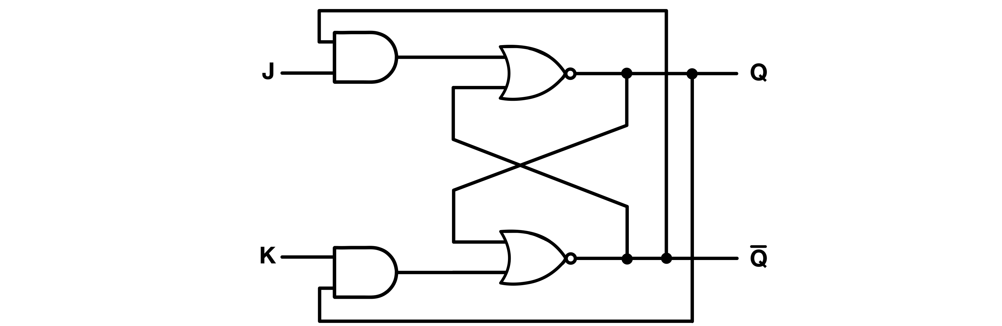
As can be seen from the diagram, the JK latch is actually an SR latch with its outputs cross-connected to its inputs using AND gates. These gates would never be HIGH at the same time, because Q and Q’ can never be HIGH simultaneously.
When J and K are both 1, the latch toggles(inverts the values of its outputs).
For example, lets start with a set state in which, Q = 1, Q’ = 0 and J = K = 0.
If J and K go HIGH at the same time ( J = K = 1), only the AND gate connecting J will go high, which will reset the SR latch (Q = 0 and Q’ = 1).
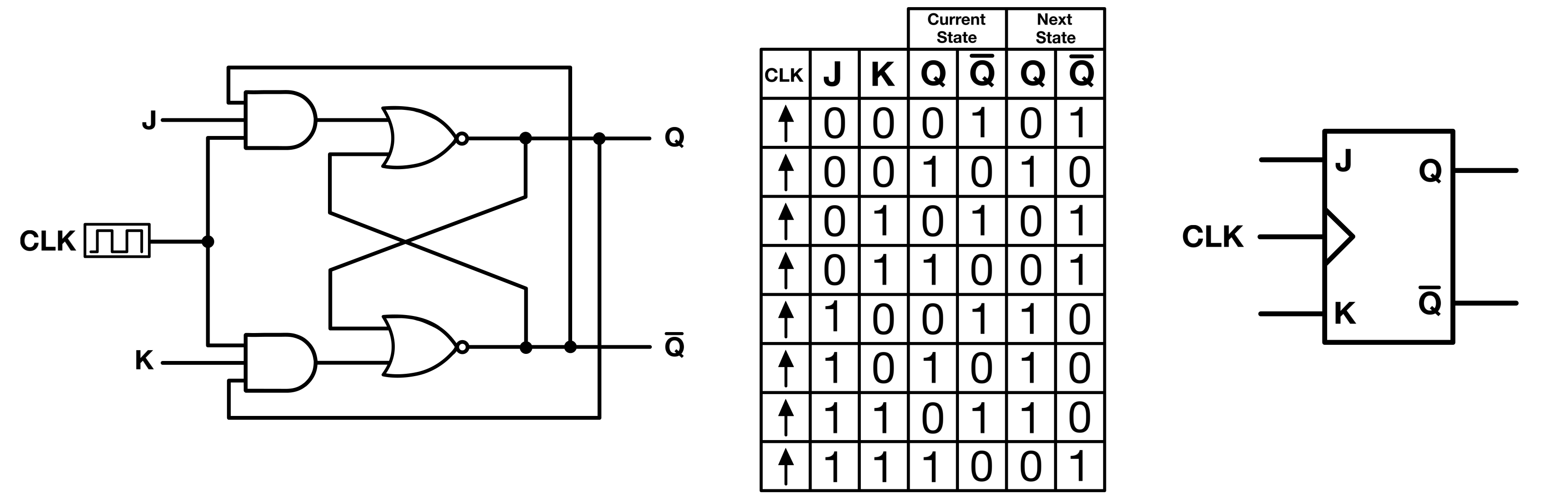
Adding a pulse detector to the JK latch turns it into a JK flip flop, as it now requires a clock for the AND gates to produce high outputs.
Fun Fact: The J and K inputs stand for Jack Kilby, the inventor of the JK flipflop.
Binary Counter
A binary counter is simply a sequential circuit that increments or decrements the value it holds at either a rising or falling edge of a clock.
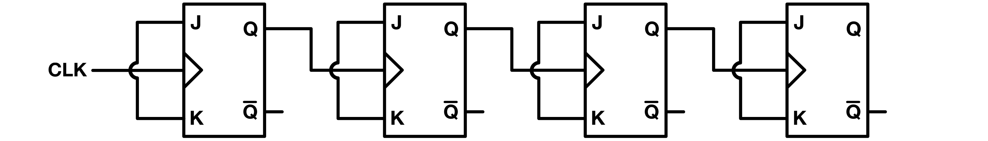
A common circuit used to implement a counter is the JK flip-flop.
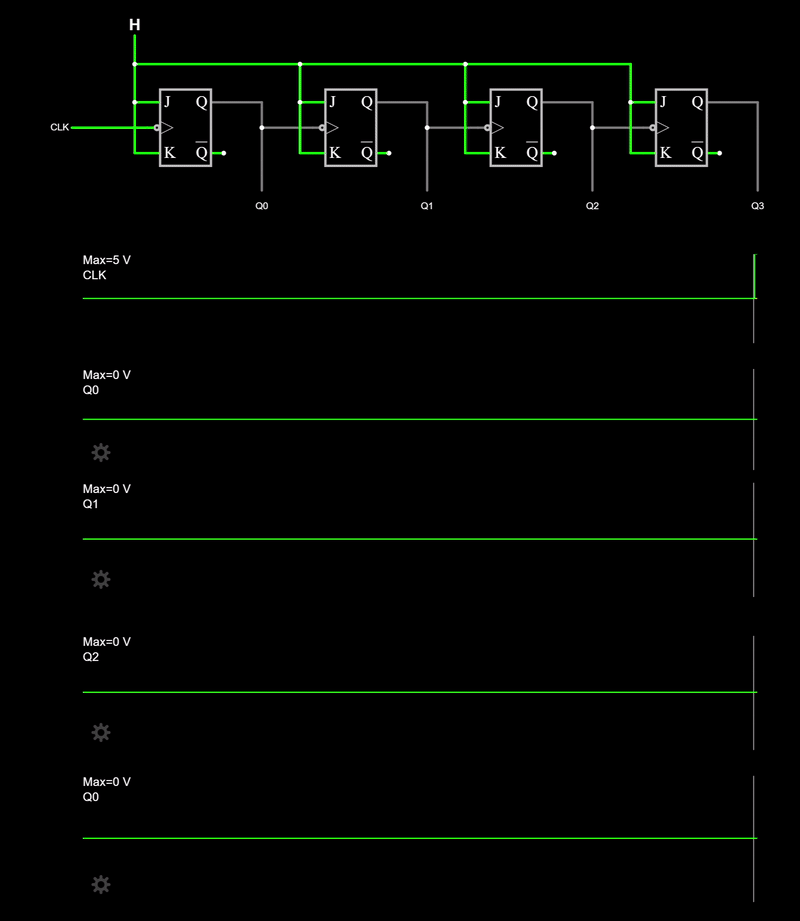
The implementation is very straightforward: Simply use several toggled(J = K = 1) JK flip flops(One per bit) sharing the same clock and feed the input of each to the next one. Naturally this same methodology can be used to divide the frequency of a signal.
Below is a Falstad simulation of the circuit above:
Program Counter
The Program Counter (PC) typically increments its content sequentially, moving from one instruction in memory at its current value/address “n” to the next address “n + 1”. However, control flow instructions such as jumps, branches, and calls can alter this sequential progression. These instructions can modify the PC’s value to an address other than “n + 1”, enabling the CPU to skip over or repeat certain sections of code based on specific conditions or explicit commands. This functionality enables the implementation of very useful operations like loops, conditional execution, and function calls.
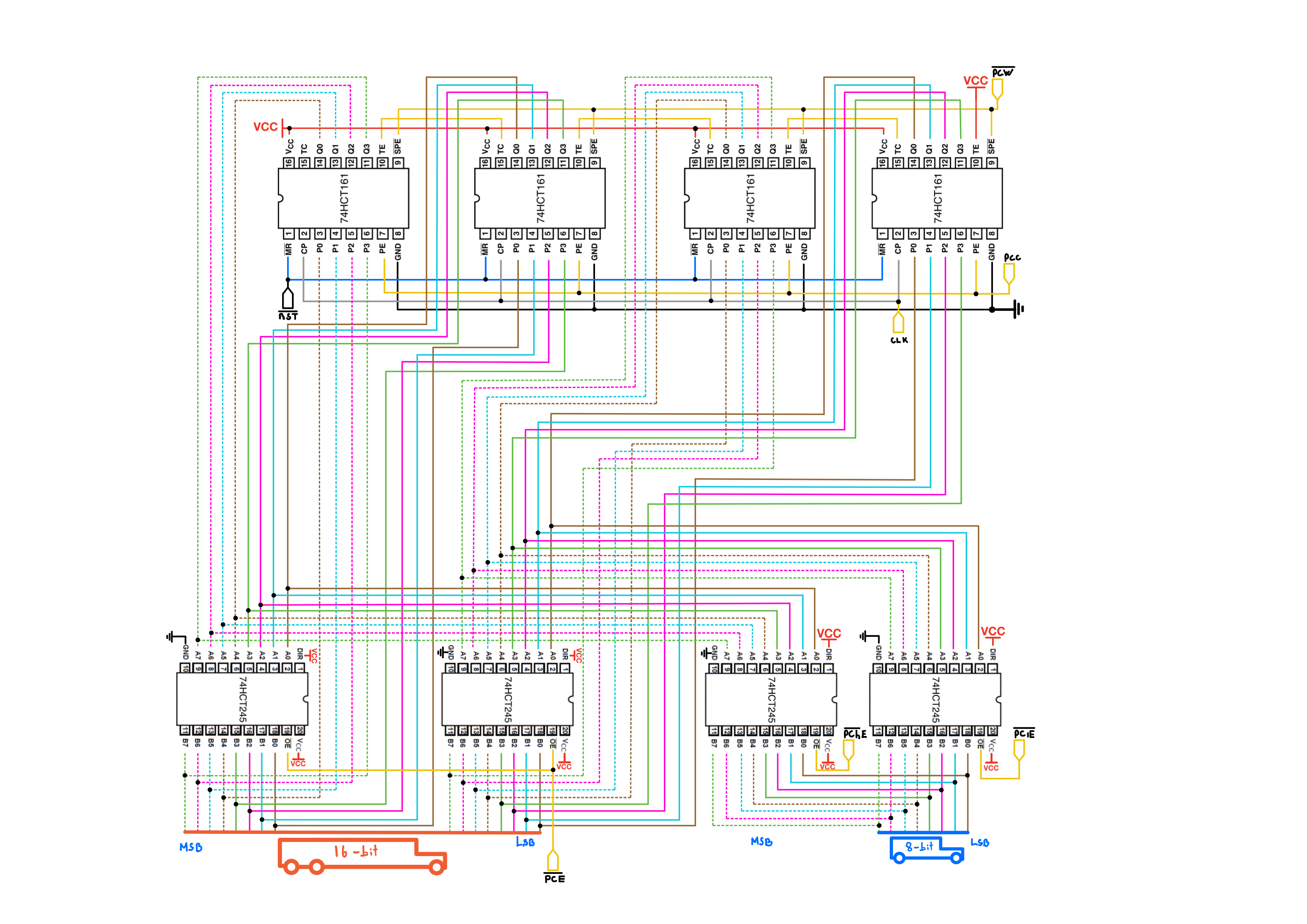
Since the CPU has a 16-bit memory bus, it naturally follows that the Program Counter should be 16-bit wide as well. The PC is made out of four cascaded 74HCT161 4-bit registers. Below are the schematic and pins description of the chip.
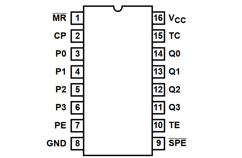
| Pin Number | Input Name | Description |
|---|---|---|
| 1 | ~MR | Clears the counters’ content when connected to Ground; inactive when connected to VCC |
| 2 | CP | Clock input |
| 3 to 6 | P0 to P6 | Data input, used to input arbitrary data to the counter |
| 7 | PE | Enables(Counts up) all flip flops in parallel |
| 8 | GND | Ground |
| 9 | ~SPE | Loads the value from pins 3 to 6 into the counter when LOW; allows normal counting when HIGH |
| 10 | TE | Enables a carry input from another counter, used in cascade configurations |
| 11 to 14 | Q0 to Q3 | Counter’s output bits |
| 15 | RCO | Ripple Clock Output, for cascading counters |
| 16 | VCC | Positive supply voltage |
Table 1: 74HCT161 Pin Configuration
74HCT161 Counter Cascading
Consider two n-bit counters to be used as a single 2n-bit counter. At first, it may seem sufficient to feed the most significant output bit of the least significant counter(C0) to the clock input of the most significant counter(C1), but it becomes obvious why this wouldn’t work with a simulation:
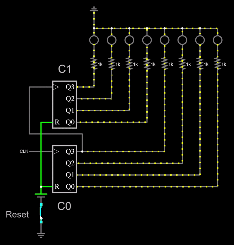
You can see that C1 increments its output every time the MSB of C0 rises, which is not desired. You want C1 to increment only when all the output bits of C0 are HIGH. In decimal, that would mean for example that all the 10s have incremented before starting incrementing the hundreds.
Here is a configuration which does exactly that. I connected a Falstad built-in 8-bit counter to the same clock as the cascaded counters to compare their outputs. The LEDs light up at approximately the same rate. I suppose the small delay comes from the circuitry of the built-in 8-bit counter.
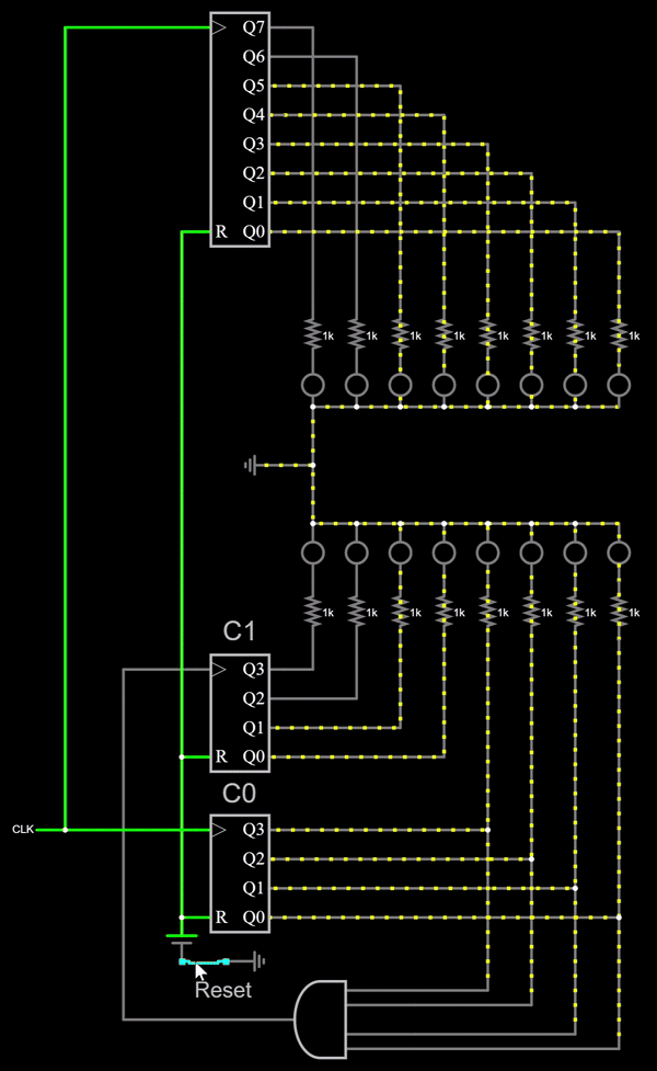
On the 74LS161, RCO is HIGH only when ENT and every single output bit of the counter are HIGH. This counting principle is the same as the one used in the Falstad simulation, except that the counters used in the simulation do not have an ENT or ENP input.
In a nutshell, to operate two 74LS161 counters, C0 and C1, in cascade: C0’s ENT can be permanently set to HIGH, while C1’s ENT can be connected to C0’s RCO.
Another very important feature of the 74HCT161 is the asynchronous reset. This is used to bring the PC to zero when the CPU powers up; independently of the clock.
Stack Pointer
The Stack Pointer too is 16-bit wide; and the reason is just because the upper portion(16 kilo bytes) of the RAM cannot be used like normal memory since the boot loader ROM overlaps this address space. An “economical” way of using this restricted memory space is by allowing it to be accessed only for stack-related operations. This way if the Stack Memory Enable ~SPE control line is not asserted, the ROM’s content would take precedence over the stack content and be addressed instead.
And since the stack memory is located on the upper half of the RAM; it is accessed from top to bottom. In other words, the Stack pointer; instead of starting pointing to memory locations from the start of the RAM(Which is typically filled with programs’ instructions) starts from the unused end/top of the RAM(0xFFFF) and decrements as more stack addresses are used.
As will be seen from the example section, practically speaking, the Stack Pointer does not need to be nearly as large as it is for such a low memory CPU. It is this wide just out of convenience.
Unlike the Program Counter, the Stack Pointer can count both up and down. The “stack” itself is a section of memory used for storing temporary data such as function call return addresses and local variables. Before the Stack Pointer changes, it typically points to the current “top” of the stack in memory. When data is “pushed” onto the stack (like a return address during a function call), it is written into memory at the address currently pointed to by the Stack Pointer. After this write operation, the Stack Pointer decrements to reflect the new top of the stack. Conversely, when data is “popped” from the stack, the Stack Pointer increments first, and then the data at the new address is read.
My stack pointer is implemented using four 74HCT191 up/down counters.
| Pin Number | Input Name | Description |
|---|---|---|
| 3, 2, 6, 7 | QA to QD | Counter’s output bits |
| 4 | ~CTEN | Enables(Counts up/down) all the flip flops |
| 5 | D/~U | Down/Up input |
| 8 | GND | Ground |
| 11 | ~LOAD | Loads the counter when LOW; allows normal counting when HIGH |
| 12 | MAX/MIN | Active LOW and goes HIGH when a circuit reaches zero in the count-down mode or reaches “15” in the count-up-mode. |
| 13 | ~RCO | Ripple Clock Output, for cascading counters |
| 14 | CLK | Clock input |
| 15, 1, 10, 9 | D0 to D3 | Data input |
| 16 | VCC | Positive supply voltage |
Table 2: 74HCT191 Pin Configuration
Checkout this nexperia datasheet for more detail on the 191’s functioning.
As mentioned in the 191’s function table, ~CEN and U/D should only be changed during the HIGH phase of the clock. The control line connected to the ~U/D pin is Active HIGH, meaning that to initiate a decrement, the ~U/D line must be set to 0 in the current cycle and kept at 0 until the next cycle where the decrements actually happens.
The 74HCT191 has an asynchronous load feature; which means that regardless of the clock’s state, the value on the counter’s input is loaded into the SP, as long as ~LOAD is LOW. Although this might not pose an issue in practice, I followed DerULF1’s guidance of NANDing the SPW (Stack Pointer Write) control line with the clock. This ensures that the Stack Pointer updates during the HIGH phase of the clock.
Program Counter And Stack Pointer Working Principle
The Program Counter normally increments sequentially, moving from one instruction to the next in the order they are stored in memory. However, a “jump” instruction disrupts this sequential flow. A jump instructs the PC to move to a different memory address, skipping over or repeating certain sections of the code based on conditions or explicit instructions. This action changes the normal flow of execution, directing the CPU to execute instructions from a different part of the program.
Unlike the Program Counter; the Stack Pointer can count both up and down. The “stack” itself is a portion of memory used for storing temporary data like function call return addresses, and local variables. Before the Stack Pointer changes, it typically points to the current “top” of the stack in memory. When data is “pushed” onto the stack (like a return address during a function call), it is written into memory at the address the Stack Pointer is currently pointing to. After this write operation, the Stack Pointer decrements to reflect the new top of the stack. Conversely, when data is “popped” from the stack, the Stack Pointer increments first, and then the data at the new address it points to is read.
Example of PC and SP working principle
Immediate instructions(The ones that handle an arbitrary number directly) in my CPU require two memory locations: One for the micro-code, and one for the number. For the sake of this example, let’s assume that all instructions take only one memory location.
; Initial Conditions:

; Let's assume the following program is loaded into memory starting from address 0x0000:
;   MOV $A, 5
;   PSH $A
;   SUB $A, 1
;   CMP $A, 0
;   PUL $A
;   JZ 0x200
;   0x200

; $PC points to the first instruction in memory at 0x0000
; The stack is empty (Points to the highest usable memory address 0xFFFF)

MOV $A, 5  ; Load 5 into register A.
; $PC now points to the next instruction (PSH $A at address 0x0001)
; $SP remains unchanged (still points to address 0xFFFF)

PSH $A ; Push the content of register A onto the stack
; $PC now points to the next instruction (SUB $A, 1 at address 0x0002)
; $SP is decremented by 1 to make space for the value pushed onto the stack and
; now points to address 0xFFFE

SUB $A, 1  ; Subtract 1 from the value in register A and store the result in
					 ; register A. So, now $A holds 4.
; $PC now points to the next instruction (CMP $A, 0 at address 0x0003)
; $SP remains unchanged (still points to address 0xFFFE)

CMP $A, 0  ; Check if A is zero
; $PC points to the next instruction (PUL $A at address 0x0004)
; $SP remains unchanged (still points to address 0xFFFE)

PUL $A; Pull the content of register A from the stack
; $PC now points to the next instruction (JZ 0x200 at address 0x0005)
; $SP is incremented by 1 as an item removed from the stack, hence going back to 0xFFFF)

JZ 0x200  ; Jump to 0x200 if the content of register A is zero
; Since $A is not zero (holds 4), $PC moves to the instruction after JZ
; $PC now points to the next instruction (at address 0x0006)
; $SP remains unchanged (still points to address 0xFFFF)

; ... The code would continue with other instructions starting here

; Address to jump to if A was zero
0x200:
; $PC would only have pointed here if $A was zero in the CMP instruction
; $SP would remain unchanged from its state before the jump
; ...This section would contain instructions specific to the case where A
; was zero.
Implementations
Program Counter
Control lines involved(5):
- |← ~PCW Program Counter Write(Jump)
- |← PCC Program Counter Count Up: Increments PC by 1
- |← ~PCE Program Counter word(16-bit) Enable
- |← ~PChE Program Counter upper/high byte enable Enable
- |← ~PClE Program Counter lower byte enable Enable
Below is the schematic of my PC module. The pair of 8-bit bus transceivers on the right enables writing either the upper or lower byte of the PC to the data bus with ~PChE and ~PClE respectively. The pair of transceivers on the left allows the counter to output its value to the 16-bit address bus in a single cycle with ~PCE. The PC can also be directly loaded from the address bus with ~PCW.
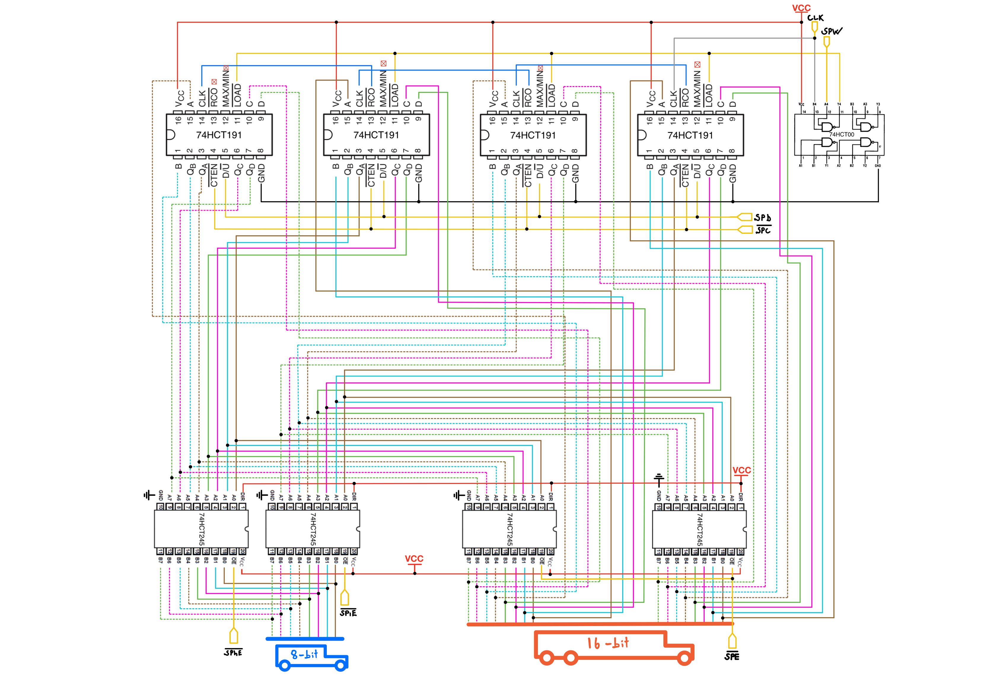
Stack Pointer
Control lines involved(6):
- |←~SPW Stack Pointer Write
- |← SPC Stack Pointer Count Enable: Increments PC by 1
- |← SPC Stack Pointer Count Direction(Up or down)
- |← ~SPE Stack Pointer word(16-bit) Enable
- |← ~SPhE Stack Pointer upper/high byte enable Enable
- |← ~SPlE Stack Pointer lower byte enable Enable
Below is the schematic of the Stack Pointer module. The pair of 8-bit bus transceivers on the left enables outputting either the upper or lower byte of the PC to the data bus with ~SPhE and ~SPlE respectively. The pair of transceivers on the right allows the SP to output its value to the 16-bit address bus in a single cycle with ~SPE.
ICS
Program Counter
4x 74HCT161, Synchronous 4-Bit Binary Counters, (Digikey, Datasheet)
4x 74HCT245, Octal Bus Transceivers With 3-State Outputs, (Digikey, Datasheet)
Stack Pointer
4x 74HCT191 Synchronous Up/Down Counters with Down/Up Mode Control(Digikey, Datasheet)
4x 74HCT245, Octal Bus Transceivers With 3-State Outputs, (Digikey, Datasheet)
«««««««««« Previous Post: Numerical Display Module
Next Post: Control Unit & Instruction Register »»»»»»»»»»
Updated: